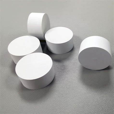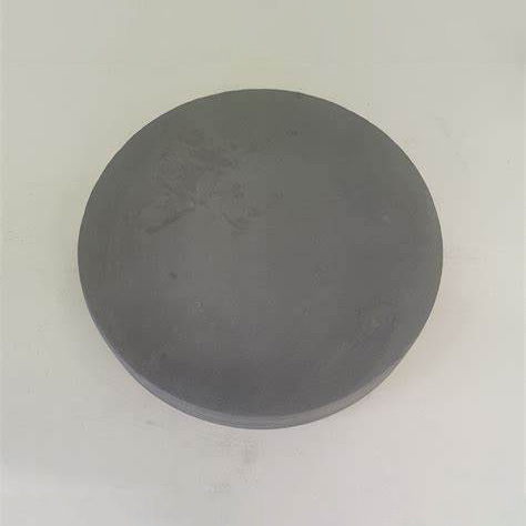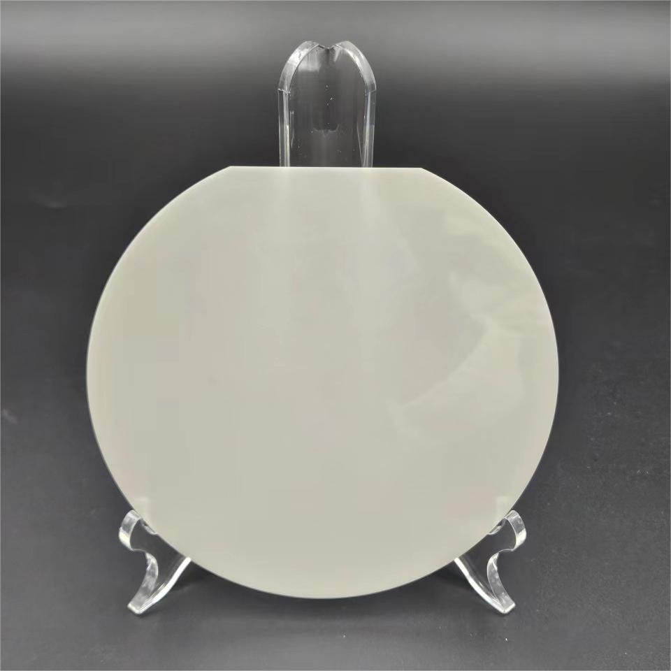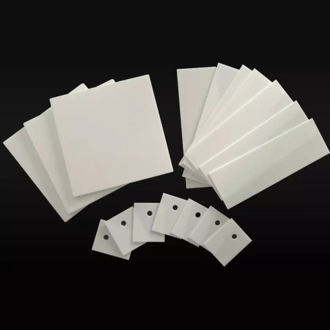
Al2O3 Wafer Alumina Ceramic Wafer
Ceramic Wafers

-
+86-17701852595 WhatsApp
-
sales@plutosemitech.com Email
Al2O3 wafers, or alumina ceramic wafers, are made of a ceramic material primarily composed of aluminum oxide (Al2O3). This material is widely used in numerous industrial fields due to its unique physical and chemical properties. This type of wafer is made by densifying powdered aluminum oxide through a high-temperature sintering process, forming a rigid substrate with a stable crystal structure. Its chemical name is aluminum oxide, which has a hexagonal crystal structure and is inert at room temperature, making it less reactive to other substances. The production of Al2O3 wafers requires precise control of material purity, size, and surface treatment to meet the needs of diverse applications.

Product Standard:
| Product Name | Purity / Method | Size | Thickness | Polishing |
| Alumina Ceramic substrate | 96% 99% 99.7% | 114.3 x 114.3mm 101.6 x 101.6mm 100 x 100mm 76.2 x 76.2mm 50 x 50mm 10 x 10mm φ50.8mm φ100mm Or others | 0.1mm 0.25mm 0.385mm 0.5mm 0.635mm 1.0mm 2.0mm Or others | Un-polished surface Single side polished Double side polished Unpolished: Ra 0.2~0.75um Polished: Ra 0.02~0.05um Best Polished: Ra<10nm |
Al2O3 Wafer Alumina Ceramic Wafer Specifications
| Substrate material | Alumina ceramic plate / substrate |
| Purity | Alumina(Al2O3) 96%, 99% and 99.7% |
| Density (g/cm3) | > 3.75 |
| Thermal conductivity (w/m.k) | > 24 |
| Thermal expansion (x10 -6 / ℃) | 6.5~7.5(20~300℃) 6.5~8.0(300~800℃) |
| Dielectric Strength (Kv/mm) | > 17 |
| Dielectric Constant (at 1MHZ) | 9~10 |
| Loss tangent (x10 -4 @1MHZ) | 4 |
| Flexural strength (N/mm2 ) | > 350 Mpa |
| Water absorption | 0% |
Al2O3 Wafer Alumina Ceramic Wafer Features
1. High Purity:
Al2O3 wafers are available in a variety of purity levels, including 96%, 99%, and 99.7%. High-purity Al2O3 wafers reduce the impact of impurities on material properties and ensure stability in high-temperature and chemical environments. For example, 99.7% Al2O3 wafers excel in high-precision applications. Their purity meets industry standards, effectively improving product reliability and service life.
2. Diverse Sizes:
Al2O3 wafers are available in a variety of sizes, including 114.3 x 114.3mm, 101.6 x 101.6mm, 100 x 100mm, 76.2 x 76.2mm, 50 x 50mm, 10 x 10mm, φ50.8mm, φ100mm, and custom sizes. These sizes meet diverse customer needs, from miniature electronic components to large industrial equipment. Al2O3 wafers offer suitable solutions.
3. Precise Thickness:
Al2O3 wafers are available in thicknesses ranging from 0.1mm to 2.0mm, with custom thicknesses available. Precise thickness control is crucial to ensuring wafer performance in diverse applications. For example, in semiconductor manufacturing, 0.1mm Al2O3 wafers can be used for high-precision insulation layers, while 2.0mm thickness is suitable for applications requiring higher mechanical strength.
4. Surface Treatment:
Al2O3 wafers are available in three surface finishes: unpolished, single-sided polished, and double-sided polished. The unpolished surface has a roughness of Ra of 0.2-0.75µm, making it suitable for applications requiring less demanding surface precision. The single-sided polished and double-sided polished surfaces have surface roughnesses of Ra 0.02-0.05µm and Ra <10nm, respectively, meeting the requirements of high-precision optical and electronic applications.
5. High Density:
Al2O3 wafers have a density exceeding 3.75g/cm³, which provides excellent mechanical strength and wear resistance. In industrial applications, high-density Al2O3 wafers can withstand greater mechanical stress and extend their service life.
6. Excellent Thermal Performance:
Al2O3 wafers have a thermal conductivity greater than 24W/m.K, and a thermal expansion coefficient of 6.5-7.5 x 10^-6/°C from 20-300°C, and 6.5-8.0 x 10^-6/°C from 300-800°C. These thermal performance parameters ensure the stability of Al2O3 wafers in high-temperature environments, enabling them to withstand thermal shock and temperature fluctuations.
7. High Insulation Performance:
Al2O3 wafers have a dielectric strength greater than 17 kV/mm, a dielectric constant of 9-10 at 1 MHz, and a loss tangent of 4 x 10^-4. These parameters demonstrate that Al2O3 wafers possess excellent insulation properties, making them suitable for high-voltage and high-frequency circuit applications.
8. High Strength and Low Water Absorption:
Al2O3 wafers have a flexural strength exceeding 350 MPa and a water absorption rate of 0%. These properties ensure they maintain excellent mechanical properties even in humid environments, without any loss of strength or performance due to water absorption.
Al2O3 Wafer Alumina Ceramic Wafer Process Flow
1. Raw Material Preparation:
Al2O3 wafer production begins with the preparation of high-purity Al2O3 raw materials. These raw materials undergo rigorous screening and purification to ensure their purity meets industry standards, providing a high-quality base material for subsequent production processes.
2. Molding Process:
Al2O3 wafer molding processes include press molding and slip casting. Press molding is suitable for producing wafers with uniform thickness and precise dimensions, while slip casting is suitable for producing wafers with complex shapes. Both processes ensure high-quality Al2O3 wafer molding.
3. Sintering Process:
The molded Al2O3 wafer undergoes high-temperature sintering. This sintering process takes place in a high-temperature furnace. Precise control of temperature and time is critical to ensuring wafer density and strength. The sintered Al2O3 wafer exhibits high density and excellent mechanical properties.
4. Surface Treatment:
The sintered Al2O3 wafer requires surface treatment, including polishing and grinding. The surface roughness of unpolished wafers ranges from Ra 0.2 to 0.75 μm, while the surface roughness of single-side polished wafers and double-side polished wafers is Ra 0.02 to 0.05 μm and Ra <10 nm, respectively. These surface treatments can meet the needs of various applications.
5. Quality Inspection:
Finally, Al2O3 wafers undergo rigorous quality inspections, including dimensional measurement, surface roughness testing, density testing, and thermal performance testing. Only wafers that pass these tests are released, ensuring their reliability and stability in applications.
Al2O3 Wafer Alumina Ceramic Wafer Application
1. Thick-Film Hybrid Integrated Circuits (HICs):
Al2O3 wafers are widely used in thick-film hybrid integrated circuits (HICs), primarily for thick-film circuits in the automotive and communications sectors. Their excellent insulation properties and thermal stability make them an ideal substrate material, capable of withstanding high voltage and high-frequency signals, ensuring stable circuit operation.
2. Die Stamping Sheets:
Al2O3 wafers are primarily used for die stamping applications such as crystal oscillators, potentiometers, refrigerators, and specialized sheets for military and medical applications. Their high hardness and wear resistance make them less susceptible to damage during the stamping process, extending the life of the die.
3. Laser Drilling Sheets:
Al2O3 wafers can be used for laser drilling. Their high-precision surface treatment and excellent thermal stability enable them to withstand the high temperatures and energies of laser processing, ensuring accurate and high-quality drilling.
4. Printer and Semiconductor Equipment:
Al2O3 wafers can be used in printers and semiconductor equipment, with sizes up to 380mm x 100mm and thicknesses ranging from 0.38mm to 1.2mm. Their high purity and excellent insulation properties make them an ideal insulating material, improving device performance and reliability.
5. High-Performance Heat Sinks:
99.6% Al2O3 wafers have a higher thermal conductivity (approximately 28W/m·K), making them more suitable for high-performance heat sinks than 96% purity Al2O3 wafers. Their excellent thermal conductivity effectively reduces device temperatures and improves heat dissipation efficiency.
Packaging and Transportation
The packaging should be able to withstand the impact, vibration, stacking and extrusion that may be encountered during transportation, while also it has to easy to load, unload and handle.
We use professional wafer box packaging. The wafer box is protected by a double layer bag, the inside is a PE bag that can be dust-proof, and the outside is a aluminum foil bag that can be isolated from the air. The two-layer bags are vacuum-packed.
We will choose carton models according to different sizes of products. And between the product and the carton filled with shock-proof EPE foam, play a comprehensive protection.
Finally choose air transport to reach the customer's hands. This allows customers in any country and region to receive the product in the fastest time.
We comply with the Material Safety Data Sheet (MSDS) rules to ensure that the products transported are free of harmful substances and will not cause environmental pollution and explosion and other possible hazards.

Enterprise Strength
Factory Area: 3000 sq
Process:
1. Shaping→2. Edge Profile→3. Lapping→4. Polishing→5. Cleaning→6. Packing→7. Transportation
Capacity:
Glass Wafer --- 30K pcs
Silicon Wafer --- 20K pcs
(Equal to 6in)

Quality Assurance
Quality inspection method: Product inspection in accordance with SEMI standard or according to customer's requirements, together with product COA.
Warranty period: In accordance with the contract requirements.
Quality system management:
●Organize production according to ISO9001 and other quality system standards.
Quality management system and measures:
●Establish a strict quality assurance system, the heads of all departments and quality engineers to ensure the coordinated operation of the quality system.
●Strengthen the quality inspection system, strengthen the process quality control
●Strict material quality control, ensure that the input materials meet the design requirements and technical specifications.
●Implement a timely filing system for technical data to ensure that all processing technical data is complete/accurate.
Quality control in the production stage:
●Production preparation stage: carefully organize relevant personnel to learn product drawings and technical rules, and improve the technical level of employees.
●Quality control of the production process: the implementation of a strict handover system, the previous step of the process to the next step of the transfer, should be detailed processing. At the same time, strengthen the quality inspection system to ensure the quality of each step of the process.
●Quality acceptance: All processes must be quality acceptance before proceeding to the next process.

Pre-sales and After-sales
Pre-sales Service
Professional technical support and commercial team to help you determine product specifications according to product use, and issue specifications.
On-purchase Service
Produce products according to the confirmed specifications and our process.
After Sale Service
We will respond to any product problems encountered by customers or process problems encountered by customers within 24 hours. We can choose from various forms of service, such as email, video conference and so on.
Plutosemi Co., Ltd. was established in 2019, headquartered in Nanhai, Foshan, focusing on the research and development, production, and sales of high-performance semiconductor materials.
Advanced production capacity: We have three major production bases in China, with a monthly production capacity of 100000 equivalent 6-inch silicon wafers and 30000 equivalent 8-inch glass wafers, ensuring stable and efficient product supply for our customers.
High quality products: We provide efficient and stable product supply innovative solutions in the fields of glass wafers, silicon polishing wafers, epitaxial wafers (EPI), silicon on insulator wafers (SOI), and more. Our silicon wafers have the characteristics of ultra-thin, ultraflat, and high-precision, which can meet the needs of various high-end applications. Our glass and quartz substrates are also renowned for their high smoothness and precise aperture design.