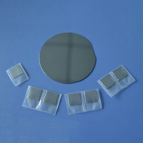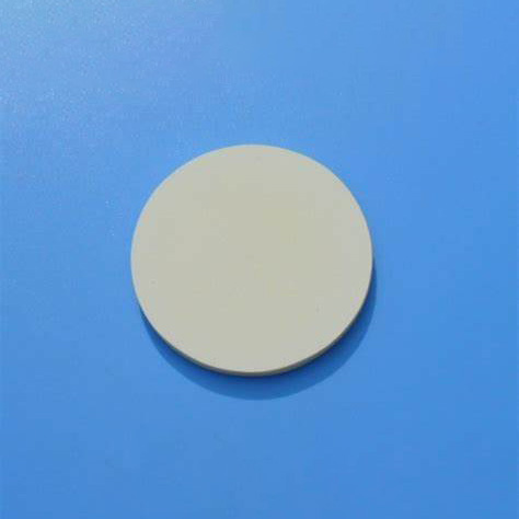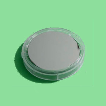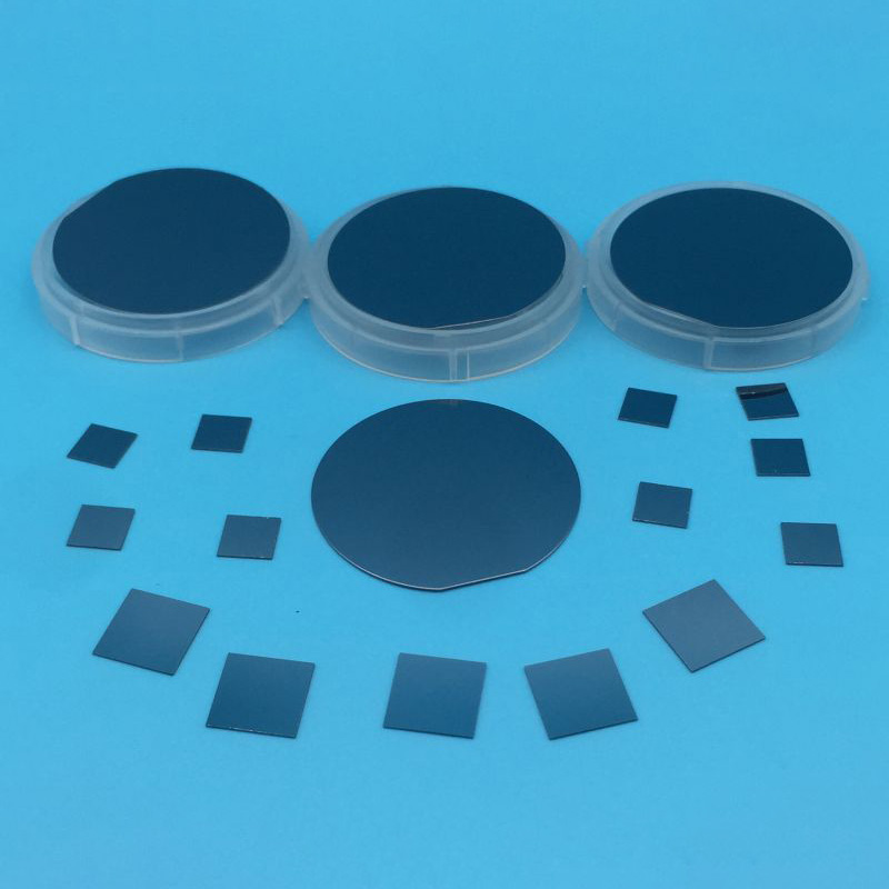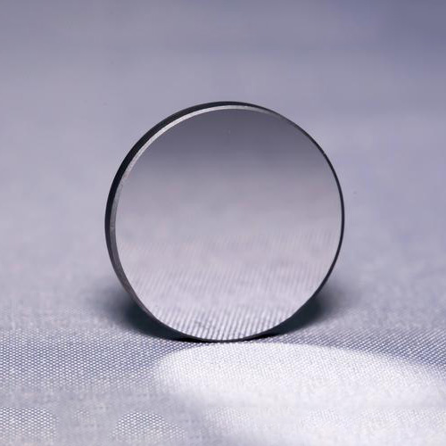
GaAs Gallium Arsenide Wafer
Compound Semiconductor Wafers

-
+86-17701852595 WhatsApp
-
sales@plutosemitech.com Email
Gallium Arsenide Wafer (GaAs wafer) is a III-V compound semiconductor material composed of gallium and arsenic. GaAs wafers usually exist in the form of single crystals. Large-sized, high-purity ingots are obtained through high-temperature crystal growth processes, and then processed into standard-sized wafers through processes such as cutting, grinding and polishing. At present, GaAs wafers are mainly divided into two types: semi-insulating and doped, which are suitable for high-end electronic and optoelectronic applications with different functional requirements.

GaAs Gallium Arsenide Wafer Specifications
| Product Name | Unit | LD Application Product Specifications | LED Application Product Specifications | Microelectronics Applications Product Specifications |
| Conductive Type | n-type | p-type/n-type | - | |
| Crystal Growth Methods | VGF | VGF | VGF | |
| Dopant | Si | Zn/Si | Undopant | |
| Diameter | inch | 2",3",4" and 6" | 2",3",4" and 6" | 2",3",4" and 6" |
| Orientation(*) | (100)±0.1° | (100)±0.5° | (100)±0.5° | |
| OF/IF | US or EJ | US or EJ | US, EJ or notch | |
| Carrier Concentration | /cm3 | (0.4-2.5)×1018 | (0.5-5)×1019 (0.4-4)×1018 | |
| Resistivity (room temperature) | ohm·cm | (1.2-9.9)×10-3 | (1.2-9.9)×10-3 | >107 |
| Electron Mobility | cm2/v·s | >1500 | 50-120/>1000 | >4000 |
| EPD | /cm2 | < 500 | < 5000 | < 5000 |
| Laser Mark | Customised to customer requirements | Customised to customer requirements | Customised to customer requirements | |
| Finished Product Thickness(*) | μm | (350-650)±25 | (350-650)±25 | (350-650)±25 |
| TTV(DSP) | μm | ≤5 | ≤5 | ≤4 |
| TTV(SSP) | μm | ≤10 | ≤10 | ≤10 |
| Warp | μm | ≤10 | ≤10 | ≤10 |
| Frontside/Backside | Side1 | Polished | Polished | Polished |
| Side2 | Polished/Etched | Polished/Etched | Polished/Etched | |
| out-of-the-box | Yes | Yes | Yes | |
| Package | Single or multiple piece cassettes | Single or multiple piece cassettes | Single or multiple piece cassettes |
* Orientation and thickness can be customised according to customers' requirements.
GaAs Gallium Arsenide Wafer Features
1. High electron mobility:
Gallium Arsenide Wafer has extremely high electron mobility, and the electron movement speed under the same electric field is much faster than that of silicon-based materials. This characteristic is due to the low effective mass of electrons in its crystal structure and the weak lattice scattering effect, which allows carriers to migrate faster in the material, thereby improving the overall electrical response speed and efficiency.
2. Excellent high-frequency response:
GaAs wafers have excellent high-frequency response capabilities and can support GHz-level signal transmission and processing. Its carrier response speed is fast and the parasitic effect is small. It can maintain stable current output under high-frequency conditions while reducing signal delay and distortion, showing dynamic performance superior to traditional semiconductor materials.
3. Good optical performance:
Gallium Arsenide Wafer has a direct bandgap structure that can efficiently emit and absorb photons. Its band structure allows the direct release of photon energy when electrons and holes recombine, which improves the luminescence efficiency. In addition, the material has a high light absorption coefficient and is suitable for building an efficient photoelectric conversion interface.
4. Low noise performance:
GaAs wafers can still maintain a low noise level under high-frequency working conditions. Its carrier scattering mechanism is weak, and thermal noise and shot noise are well controlled, which helps to improve the signal-to-noise ratio of the device. The low internal defect density of the material also helps to suppress unexpected electronic fluctuations and improve the overall signal stability.
5. High output power capability:
GaAs wafers have strong current carrying capacity and high breakdown voltage. Its crystal structure is stable and can withstand high electric field strength without failure, so it can operate stably under high power conditions. The thermal conductivity of the material is also good, which helps to dissipate heat and extend the service life of the device.
6. Good linearity and stability:
Gallium Arsenide Wafer shows good electrical linearity and thermal stability over a wide temperature range. Its carrier concentration changes little with temperature, and the resistivity curve is smooth, which helps to reduce the electrical parameter drift caused by environmental changes, thereby ensuring the reliability and consistency of the long-term operation of the device.
7. Controllable doping performance:
GaAs wafers can be doped with different elements (such as Si, Ge, and Zn) to adjust their conductivity and carrier concentration. The doping uniformity during crystal growth is good and the interface state density is low, which is conducive to the realization of high-performance and high-consistency semiconductor devices to meet diverse design requirements.
8. Diversified crystal types:
Gallium Arsenide Wafer can be divided into two categories according to its use: semi-insulating type and doped type. The semi-insulating type has an extremely low background carrier concentration and is suitable for high-frequency passive substrates; while the doped type regulates the conductivity by introducing specific impurity elements to meet the manufacturing needs of active devices and optoelectronic devices.
GaAs Gallium Arsenide Wafer Process Flow
1. Raw material synthesis:
The production of Gallium Arsenide Wafer begins with the synthesis of high-purity raw materials. Gallium and arsenic are chemically reacted in a high-temperature and high-pressure reactor to form polycrystalline gallium arsenide. Since arsenic has a high vapor pressure at high temperatures, the synthesis process needs to be carried out under specific high-pressure conditions to ensure the smooth progress of the reaction.
2. Single crystal growth:
Growing single crystals from polycrystalline gallium arsenide is one of the key steps. Common methods include horizontal Bridgman, vertical gradient freeze (VGF) and liquid encapsulated Czochralski (LEC). Among them, the LEC method is currently the main method for producing high-purity single crystal gallium arsenide. By sealing the gallium arsenide melt in glass at high temperature, dislocations are prevented during crystal growth.
3. Wafer cutting and grinding:
After the single crystal is grown, it needs to be cut into thin slices, namely wafers. Diamond saw blades are usually used for cutting. The surface of the wafer after cutting is relatively rough, and grinding is required to remove the damage layer generated during the cutting process and make the wafer surface smoother.
4. Cleaning and polishing:
The surface of the Gallium Arsenide Wafer after grinding may still have impurities and tiny defects, so strict cleaning and polishing are required. The cleaning process usually includes soaking in a chemical solution to remove surface residues. Polishing uses a special polishing liquid to mechanically polish the wafer surface to achieve extremely high flatness and finish, which is crucial for subsequent microelectronic device manufacturing.
5. Wafer inspection and packaging:
Finally, the processed Gallium Arsenide Wafer is inspected to ensure that its quality and performance meet the requirements. The inspection content includes the integrity of the crystal, the flatness of the surface, the impurity content, etc. Wafers that pass the inspection will be packaged in a dedicated container to prevent damage during transportation and storage.
GaAs Gallium Arsenide Wafer Application
1. RF and microwave devices:
Gallium Arsenide Wafer is widely used in the manufacture of RF and microwave devices, such as transistors such as MESFET and HEMT. Its high electron mobility and low noise characteristics make it play a key role in 5G base stations, radars and satellite communication equipment, improving high-frequency signal processing capabilities.
2. Optoelectronic devices:
GaAs wafers are widely used in the manufacture of LEDs, laser diodes and photodetectors due to their direct bandgap characteristics. They have high luminous efficiency and fast response speed, and are suitable for a variety of optoelectronic applications such as display, lighting, fiber-optic communication and sensing.
3. Power amplifiers:
Gallium Arsenide Wafer has high breakdown voltage and excellent power handling capabilities, and is often used to manufacture RF power amplifiers. Such amplifiers are widely used in mobile communications, Wi-Fi modules and military communication equipment to ensure stable and efficient signal transmission.
4. Infrared detectors:
GaAs wafers can be used to manufacture infrared detectors, especially in the near-infrared band. Its high sensitivity and fast response capabilities make it widely used in security monitoring, thermal imaging and industrial detection.
5. Semiconductor integrated circuits:
Gallium Arsenide Wafer can be used to manufacture high-frequency analog and digital integrated circuits. Its excellent high-frequency characteristics and low parasitic effects give it obvious advantages in high-speed computing, RF front-ends and application-specific integrated circuits (ASICs).
6. Solar cells:
GaAs wafers, as high-efficiency photovoltaic materials, are used to manufacture space solar panels. It has high photoelectric conversion efficiency and strong radiation resistance, and is particularly suitable for use in the aerospace field, providing stable energy for satellites and deep space probes.
Packaging and Transportation
The packaging should be able to withstand the impact, vibration, stacking and extrusion that may be encountered during transportation, while also it has to easy to load, unload and handle.
We use professional wafer box packaging. The wafer box is protected by a double layer bag, the inside is a PE bag that can be dust-proof, and the outside is a aluminum foil bag that can be isolated from the air. The two-layer bags are vacuum-packed.
We will choose carton models according to different sizes of products. And between the product and the carton filled with shock-proof EPE foam, play a comprehensive protection.
Finally choose air transport to reach the customer's hands. This allows customers in any country and region to receive the product in the fastest time.
We comply with the Material Safety Data Sheet (MSDS) rules to ensure that the products transported are free of harmful substances and will not cause environmental pollution and explosion and other possible hazards.

Enterprise Strength
Factory Area: 3000 sq
Process:
1. Shaping→2. Edge Profile→3. Lapping→4. Polishing→5. Cleaning→6. Packing→7. Transportation
Capacity:
Glass Wafer --- 30K pcs
Silicon Wafer --- 20K pcs
(Equal to 6in)

Quality Assurance
Quality inspection method: Product inspection in accordance with SEMI standard or according to customer's requirements, together with product COA.
Warranty period: In accordance with the contract requirements.
Quality system management:
●Organize production according to ISO9001 and other quality system standards.
Quality management system and measures:
●Establish a strict quality assurance system, the heads of all departments and quality engineers to ensure the coordinated operation of the quality system.
●Strengthen the quality inspection system, strengthen the process quality control
●Strict material quality control, ensure that the input materials meet the design requirements and technical specifications.
●Implement a timely filing system for technical data to ensure that all processing technical data is complete/accurate.
Quality control in the production stage:
●Production preparation stage: carefully organize relevant personnel to learn product drawings and technical rules, and improve the technical level of employees.
●Quality control of the production process: the implementation of a strict handover system, the previous step of the process to the next step of the transfer, should be detailed processing. At the same time, strengthen the quality inspection system to ensure the quality of each step of the process.
●Quality acceptance: All processes must be quality acceptance before proceeding to the next process.

Pre-sales and After-sales
Pre-sales Service
Professional technical support and commercial team to help you determine product specifications according to product use, and issue specifications.
On-purchase Service
Produce products according to the confirmed specifications and our process.
After Sale Service
We will respond to any product problems encountered by customers or process problems encountered by customers within 24 hours. We can choose from various forms of service, such as email, video conference and so on.
Plutosemi Co., Ltd. was established in 2019, headquartered in Nanhai, Foshan, focusing on the research and development, production, and sales of high-performance semiconductor materials.
Advanced production capacity: We have three major production bases in China, with a monthly production capacity of 100000 equivalent 6-inch silicon wafers and 30000 equivalent 8-inch glass wafers, ensuring stable and efficient product supply for our customers.
High quality products: We provide efficient and stable product supply innovative solutions in the fields of glass wafers, silicon polishing wafers, epitaxial wafers (EPI), silicon on insulator wafers (SOI), and more. Our silicon wafers have the characteristics of ultra-thin, ultraflat, and high-precision, which can meet the needs of various high-end applications. Our glass and quartz substrates are also renowned for their high smoothness and precise aperture design.