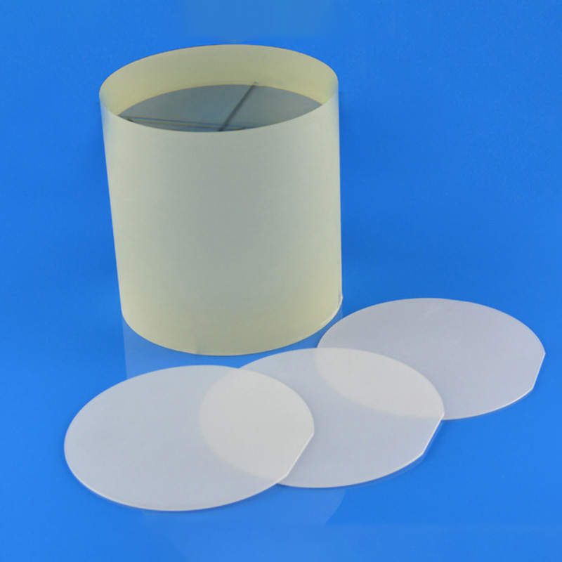
Optical Grade LiNbO3 Lithium Niobate Wafer
Compound Semiconductor Wafers

-
+86-17701852595 WhatsApp
-
sales@plutosemitech.com Email
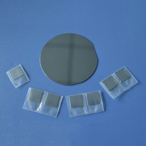
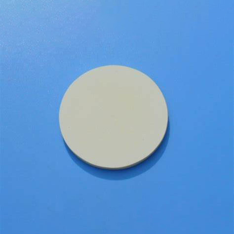
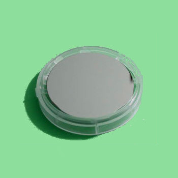
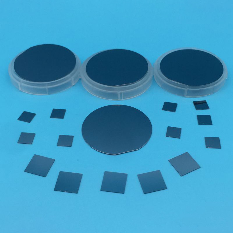
Lithium Niobate wafers are functional wafer materials made from optical-grade lithium niobate single crystals through directional cutting, precision grinding, and ultra-precision polishing. Compared to conventional functional crystals, they possess stable ferroelectric properties, significant electro-optic and acousto-optic effects, and highly consistent refractive index performance in the visible to near-infrared wavelength range, making them indispensable in high-precision optoelectronic systems. These wafers are available in white or black substrates, covering various diameters from 2 inches to 4 inches, and are manufactured with strict control over thickness, TTV, BOW, and WARP to ensure excellent flatness and repeatability during micro-nano processing and device integration.
During the manufacturing process, Lithium Niobate wafers can be precisely oriented along multiple axes such as X, Y, and Z, with orientation and thickness tolerances controlled within the micrometer range, helping to stabilize their intrinsic physical properties. Single-sided or double-sided polishing processes achieve sub-nanometer surface roughness, coupled with low surface defect density and cleanliness control, meeting the stringent requirements for interface quality in high-end optical and microelectronic processes. Through optical doping schemes with Mg, Fe, Zn, or MgO, the wafers can be further optimized for specific needs such as photorefractive suppression and optical loss control, making them more reliable in high-power and high-stability applications.

Optical Grade LiNbO3 Lithium Niobate Wafer Specifications
Optical Grade LiNbO3 Wafer
| Parameter | Specification |
| Material | Optical Grade LiNbO₃ Wafers (White or Black) |
| Diameter | 2inch/3inch/4inch |
| Diameter Tolerance | ±0.03mm |
| Curie Temp | 1142±0.2℃ |
| Cutting Angle | X/Y/Z etc. |
| Tol(±) | < 0.20 mm ±0.005mm |
| Thickness | 0.18 ~ 0.5mm or more |
| Primary Flat | 16mm/22mm /32mm |
| TTV | < 3μm |
| BOW | -30 |
| WARP | < 40μm |
| Orientation Flat | All available |
| Surface Type | Single Side Polished(SSP) /Double Sides Polished(DSP) |
| Polished side Ra | < 0.5nm |
| S/D | 20/10 |
| Edge Criteria | R=0.2mm C-type or Bullnose |
| Quality | Free of crack (bubbles and inclusions) |
| Optical doped | Mg/Fe/Zn/MgO etc. for optical grade |
| Wafer Surface Criteria | Refractive index No=2.2878/Ne=2.2033 @632nm wavelength |
| Contamination None | |
| Particles @>0.3 μm ≤30 | |
| Scratch , Chipping None | |
| Defect No edge cracks, scratches, saw marks, stains | |
| Packing | 25pcs per box |
SAW Grade Lithium Niobate Wafers
| Parameter | Specification |
| Material | LiNbO3 wafers (White or Black) |
| Diameter | 3inch/4inch/inch LN wafer & 8inch under R/D |
| Diameter Tolerance | ±0.03mm |
| Curie Temp | 1142±2.0℃ |
| Cutting Angle | X/Y/Z/Y36/Y41/Y64/Y128/etc. |
| Tol(±) | < 0.20 mm |
| Thickness | 0.18 ~ 0.5mm or more |
| Primary Flat | 22mm /32mm /42.5mm /57.5mm |
| LTV (5mmx5mm) | < 1μm |
| TTV | < 3μm |
| BOW | -30 |
| WARP | < 40μm |
| PLTV(<0.5um)<> | ≥95%(5mm*5mm) |
| Orientation Flat | All available |
| Surface Type | Single Side Polished(SSP) /Double Sides Polished(DSP) |
| Polished side Ra | < 0.5nm |
| Back Side Criteria | General is 0.2-0.5μm or as customized |
| Edge Criteria | R=0.2mm or Bullnose |
| Wafer Surface Criteria | Transmissivity general:5.9x10⁻¹¹ |
| Contamination None | |
| Particles @ > 0.3 μm ≤30 | |
| Scratch , Chipping None | |
| Defect No edge cracks, scratches, saw marks, stains | |
| Packing | 25pcs per box |
Optical grade LiNbO3 wafers SLN CLN
| Parameter | Specification |
| Material | Optical Grade LiNbO3 Wafers (White or Black) |
| Diameter | 2inch/3inch/4inch |
| Diameter Tolerance | ±0.03mm |
| Curie Temp | 1142±0.7℃ |
| Cutting Angle | X/Y/Z etc. |
| Tol(±) | < 0.20 mm ±0.005mm |
| Thickness | 0.18 ~ 0.5mm or more |
| Primary Flat | 16mm/22mm /32mm |
| TTV | < 3μm |
| BOW | -30 |
| WARP | < 40μm |
| Orientation Flat | All available |
| Surface Type | Single Side Polished(SSP) /Double Sides Polished(DSP) |
| Polished side Ra | < 0.5nm |
| S/D | 10月20日 |
| Edge Criteria | R=0.2mm C-type or Bullnose |
| Quality | Free of crack (bubbles and inclusions) |
| Optical doped | Mg/Fe/Zn/MgO etc. for optical grade LN < wafers per requested |
| Wafer Surface Criteria | Refractive index No=2.2878/Ne=2.2033 @632nm wavelength/prism coupler method. |
| Contamination None | |
| Particles @ > 0.3 μm ≤30 | |
| Scratch , Chipping None | |
| Defect No edge cracks, scratches, saw marks, stains | |
| Packing | 25pcs per box |
Optical Grade LiNbO3 Lithium Niobate Wafer Features
1. Stable Electro-Optical Properties
The Lithium Niobate wafer possesses stable electro-optical coefficients, with refractive indices of No=2.2878 and Ne=2.2033 at a wavelength of 632nm, ensuring highly controllable phase changes during electric field modulation. Its Curie temperature is 1142±0.2℃, maintaining stable crystal polarization even under high-temperature processing or long-term operation, preventing performance drift.
2. Ultra-High Flatness
The wafer has a TTV of less than 3μm, WARP controlled within 40μm, and a BOW value of approximately -30μm, ensuring excellent contact during photolithography and deposition processes. Precise flatness control effectively reduces the risk of stress concentration, providing a stable foundation for high-consistency device manufacturing.
3. Surface Precision
The polished surface has an Ra of less than 0.5nm, S/D grade of 20/10, and is free of scratches, saw marks, and contamination residue. This level of surface quality significantly reduces scattering loss, improves optical interface coupling efficiency, and meets the interface quality requirements of high-sensitivity optical systems.
4. Flexible Orientation
The wafer supports various cutting angles, including X, Y, and Z axes, and offers 16mm, 22mm, and 32mm primary orientation edges, with strictly controlled orientation errors. Multiple orientation options facilitate design based on different material properties, enhancing the design freedom and consistency of device parameters.
5. Controllable Doping
Optical-grade doping methods using Mg, Fe, Zn, or MgO can adjust the photorefractive threshold and light absorption characteristics. The doping concentration and uniformity have been verified, helping to suppress performance degradation under high light intensity conditions and improve long-term operational stability.
Optical Grade LiNbO3 Lithium Niobate Wafer Process Flow
Raw material selection:
Plutosemi strictly selects high-purity LiNbO₃ raw materials when producing Optical Grade LiNbO₃ Wafer. Through advanced testing equipment, the purity of the raw materials is ensured to reach more than 99.99%, laying the foundation for subsequent high-quality production.
Crystal growth:
Advanced crystal growth techniques such as Czochralski or zone melting are used to accurately control the growth process of the crystal. By optimizing growth parameters such as temperature, pressure and growth rate, high-quality crystal growth is ensured and crystal defects are reduced.
Cutting and grinding:
Use high-precision cutting equipment to cut according to the size and cutting angle required by the customer. The cut wafers are finely ground to ensure that the dimensional accuracy and surface flatness meet industry standards.
Polishing:
Advanced polishing process is used to polish the surface of LiNbO3 wafer on one side or both sides. By optimizing polishing parameters, the surface roughness (Ra) is ensured to be less than 0.5nm, which meets the requirements of high-end optical applications.
Quality inspection:
During the production process, each LiNbO3 wafer is strictly inspected for quality. The inspection contents include dimensional accuracy, surface quality, optical performance, etc. Through strict quality control, we ensure that each wafer can meet the high quality requirements of customers.
Customized processing:
Customized processing services are provided according to the special needs of customers. Including adjusting the size, thickness, cutting angle and other parameters of LiNbO3 wafer to ensure that the product can perfectly adapt to the customer's equipment and applications.
Optical Grade LiNbO3 Lithium Niobate Wafer Application
1. Optical Communication
Lithium Niobate wafers are one of the key functional materials in high-speed optical communication systems, primarily used to construct highly stable optical signal modulation and control structures. Its crystal exhibits a consistent refractive index distribution within the operating wavelength range, helping to maintain stable signal phase and intensity output. Precise cutting orientation and thickness control enable highly consistent optical signal response behavior, allowing communication systems to maintain low bit error rates and reliable signal integrity under long-term operation, suitable for communication architectures requiring high stability.
2. Integrated Optics
In integrated optical systems, Lithium Niobate wafers serve as a fundamental substrate material, providing stable support for various optical structures. Its excellent geometric consistency and surface quality make it easier to control dimensional deviations during microfabrication processes, thereby improving overall integration accuracy. The wafer maintains stable flatness even after multiple processing steps, helping to reduce coupling errors between structures and meeting the requirements of high-density optical circuit layouts and system-level consistency.
3. Laser Systems
Lithium Niobate wafers are widely used in laser-related optical control structures, especially suitable for systems requiring long-term stable operation. Its low crystal defect density and high optical uniformity effectively reduce unnecessary energy loss during laser transmission and modulation. Through appropriate doping and process control, the wafer maintains stable optical response characteristics even under high light intensity conditions, providing a reliable foundation for system operation.
4. Acousto-optic Devices
In acousto-optic device structures, Lithium Niobate wafers serve as the core medium for the interaction of acoustic and optical waves. The wafer's stable dimensions and precise orientation ensure consistent response behavior under different frequencies. Good processing consistency helps reduce performance deviations during the acousto-optic conversion process, allowing the device to maintain predictable operating conditions under continuous operation or mass production, suitable for signal processing systems requiring high response stability.
5. Precision Sensing
Lithium Niobate wafers are used as functional substrates in various precision sensing structures. Their stable physical parameters help obtain repeatable and calibratable detection results. The wafer's high surface cleanliness and good edge integrity reduce structural risks during assembly and packaging. Supported by stable material properties, the sensing system maintains measurement consistency even under complex environmental conditions, meeting the requirements of detection applications requiring high reliability and long-term stability.
Optical Grade LiNbO3 Lithium Niobate Wafer FAQ
Q: How is the dimensional consistency of Lithium Niobate wafers ensured?
A: The wafer diameter tolerance is controlled within ±0.03mm, and the thickness is selectable from 0.18 to 0.5mm and above. Both thickness and orientation tolerances are controlled at the micrometer level. Combined with a rigorous inspection process, this ensures consistent dimensions and physical properties between batches.
Q: How does polishing quality affect practical use?
A: The polished surface Ra is less than 0.5nm, which significantly reduces light scattering and interface loss. Stable surface quality helps improve device repeatability and reduces yield fluctuations caused by surface defects in subsequent processes.
Q: Do you support double-sided polishing specifications?
A: Both SSP (single-sided polishing) and DSP (double-sided polishing) surface types are supported. Double-sided polishing provides better flatness and thickness consistency when double-interface processing or highly symmetrical structures are required, making it suitable for high-precision device design.
Q: How is the wafer cleanliness standard controlled?
A: The surface is free of contamination residue, with no more than 30 particles larger than 0.3μm, and no edge cracks or notches. This standard helps reduce process risks and improve overall reliability.
Q: Does packaging and transportation affect performance?
A: We use a 25-wafer individual box packaging solution, combined with shockproof and anti-contamination designs, to effectively maintain the surface and structural integrity of the wafers during transportation and storage, ensuring that performance is unaffected when they reach the customer.
Packaging and Transportation
The packaging should be able to withstand the impact, vibration, stacking and extrusion that may be encountered during transportation, while also it has to easy to load, unload and handle.
We use professional wafer box packaging. The wafer box is protected by a double layer bag, the inside is a PE bag that can be dust-proof, and the outside is a aluminum foil bag that can be isolated from the air. The two-layer bags are vacuum-packed.
We will choose carton models according to different sizes of products. And between the product and the carton filled with shock-proof EPE foam, play a comprehensive protection.
Finally choose air transport to reach the customer's hands. This allows customers in any country and region to receive the product in the fastest time.
We comply with the Material Safety Data Sheet (MSDS) rules to ensure that the products transported are free of harmful substances and will not cause environmental pollution and explosion and other possible hazards.

Enterprise Strength
Factory Area: 3000 sq
Process:
1. Shaping→2. Edge Profile→3. Lapping→4. Polishing→5. Cleaning→6. Packing→7. Transportation
Capacity:
Glass Wafer --- 30K pcs
Silicon Wafer --- 20K pcs
(Equal to 6in)

Quality Assurance
Quality inspection method: Product inspection in accordance with SEMI standard or according to customer's requirements, together with product COA.
Warranty period: In accordance with the contract requirements.
Quality system management:
●Organize production according to ISO9001 and other quality system standards.
Quality management system and measures:
●Establish a strict quality assurance system, the heads of all departments and quality engineers to ensure the coordinated operation of the quality system.
●Strengthen the quality inspection system, strengthen the process quality control
●Strict material quality control, ensure that the input materials meet the design requirements and technical specifications.
●Implement a timely filing system for technical data to ensure that all processing technical data is complete/accurate.
Quality control in the production stage:
●Production preparation stage: carefully organize relevant personnel to learn product drawings and technical rules, and improve the technical level of employees.
●Quality control of the production process: the implementation of a strict handover system, the previous step of the process to the next step of the transfer, should be detailed processing. At the same time, strengthen the quality inspection system to ensure the quality of each step of the process.
●Quality acceptance: All processes must be quality acceptance before proceeding to the next process.

Pre-sales and After-sales
Pre-sales Service
Professional technical support and commercial team to help you determine product specifications according to product use, and issue specifications.
On-purchase Service
Produce products according to the confirmed specifications and our process.
After Sale Service
We will respond to any product problems encountered by customers or process problems encountered by customers within 24 hours. We can choose from various forms of service, such as email, video conference and so on.
Plutosemi Co., Ltd. was established in 2019, headquartered in Nanhai, Foshan, focusing on the research and development, production, and sales of high-performance semiconductor materials.
Advanced production capacity: We have three major production bases in China, with a monthly production capacity of 100000 equivalent 6-inch silicon wafers and 30000 equivalent 8-inch glass wafers, ensuring stable and efficient product supply for our customers.
High quality products: We provide efficient and stable product supply innovative solutions in the fields of glass wafers, silicon polishing wafers, epitaxial wafers (EPI), silicon on insulator wafers (SOI), and more. Our silicon wafers have the characteristics of ultra-thin, ultraflat, and high-precision, which can meet the needs of various high-end applications. Our glass and quartz substrates are also renowned for their high smoothness and precise aperture design.