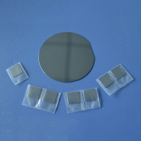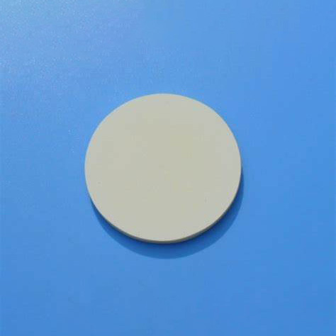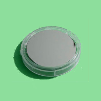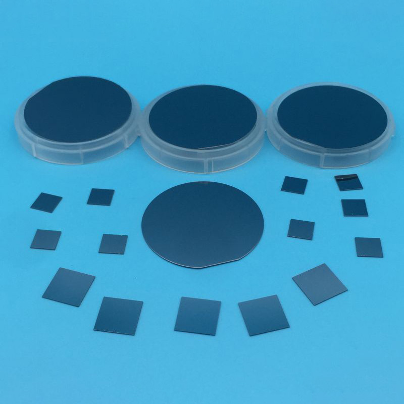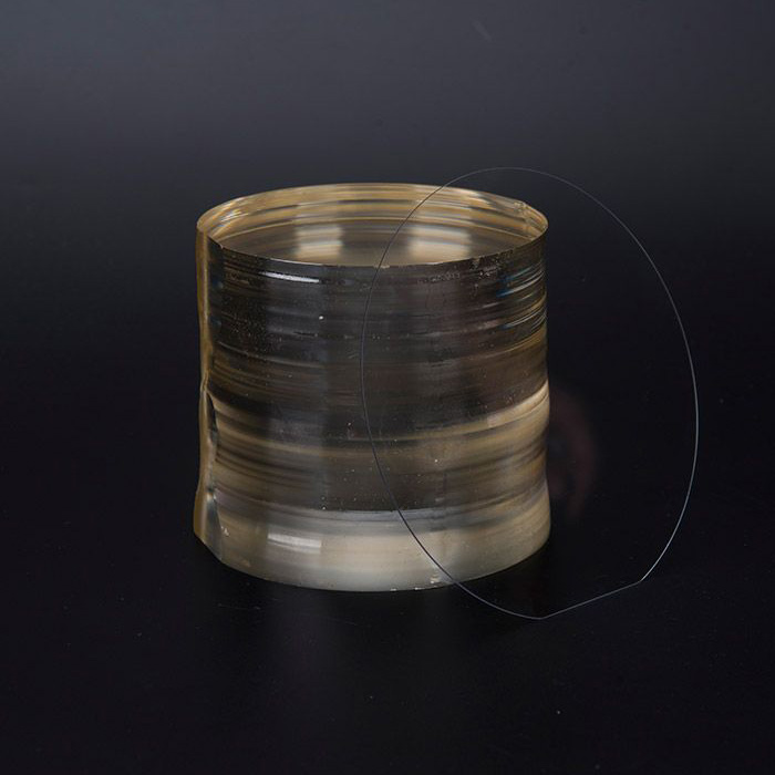
Optical Grade Lithium Tantalate Wafer
Compound Semiconductor Wafers

-
+86-17701852595 WhatsApp
-
sales@plutosemitech.com Email
Lithium Tantalate (LT) is a material with a unique crystal structure and a chemical formula of LiTaO₃. It is a monoclinic compound with a stable crystal structure and excellent physical and chemical properties. Lithium Tantalate Wafe has attracted much attention in materials science, and its crystal structure gives it good piezoelectricity, pyroelectricity and optical properties. The preparation of this material requires strict control of crystal growth conditions to ensure its high quality and high performance. It plays an important role in many high-tech fields and is one of the indispensable key materials for modern science and technology.

Optical Grade Lithium Tantalate Wafer Specifications
Fe doped LT Wafers
| Parameter | Specification |
| Material | LiTaO3 wafers(White or Black &Fe doped) |
| Diameter | 3inch/4inch/6inch |
| Diameter Tolerance | ±0.03mm |
| Curie Temp | 603±2℃ |
| Cutting Angle | X/Y/Z/X112Y/Y36/Y42/Y48/etc |
| Tol(±) | < 0.20 mm |
| Thickness | 0.18 ~ 0.5mm or more |
| Primary Flat | 22mm /32mm /42.5mm /57.5mm |
| LTV (5mmx5mm) | < 1μm |
| TTV | < 3μm |
| BOW | -30 |
| WARP | < 40μm |
| PLTV(<0.5um)<> | ≥95%(5mm*5mm) |
| Orientation Flat | All available |
| Surface Type | Single Side Polished(SSP) /Double Sides Polished(DSP) |
| Polished side Ra | < 0.5nm |
| Back Side Criteria | General is 0.2-0.5μm or as customized |
| Edge Criteria | R=0.2mm or Bullnose |
| Fe doped | Fe doped for saw grade LN < wafers |
| Wafer Surface Criteria | Transmissivity general: 5.9x10⁻¹¹ < s<2.0*10-11 |
| Contamination None | |
| Particles @>0.3 μm ≤30 | |
| Scratch, Chipping None | |
| Defect No edge cracks, scratches, saw marks, stains | |
| Packing | 25pcs per box |
Optical Grade Lithium Tantalate Wafers
| Parameter | Specification |
| Material | LiTaO3 wafers(White or Black) |
| Diameter | 2inch/3inch/4inch |
| Diameter Tolerance | ±0.03mm |
| Curie Temp | 603±2℃ |
| Cutting Angle | X/Y/Z etc. |
| Tol(±) | < 0.20 mm |
| Thickness | 0.18 ~ 0.5mm or more |
| Primary Flat | 16mm/22mm /32mm |
| TTV | < 3μm |
| BOW | -30 |
| WARP | < 40μm |
| Surface Type | Single Side Polished(SSP) /Double Sides Polished(DSP) |
| Polished side Ra | < 0.5nm |
| Back Side Criteria | General is 0.2-0.5μm or as customized |
| Edge Criteria | R=0.2mm or Bullnose |
| Optical doped | Zn/MgO etc. |
| Wafer Surface Criteria | Contamination None |
| Particles @>0.3 μm ≤30 | |
| Scratch, Chipping None | |
| Defect No edge cracks, scratches, saw marks, stains | |
| Packing | 25pcs per box |
SAW Grade Lithium Tantalate Wafers
| Parameter | Specification |
| Material | LiTaO3 wafers |
| Diameter | 3inch/4inch/6inch |
| Diameter Tolerance | ±0.03mm |
| Curie Temp | 603±2℃ |
| Cutting Angle | X/Y/Z/X112Y/Y36/Y42/Y48/etc. |
| Tol(±) | < 0.20 mm |
| Thickness | 0.18 ~ 0.5mm or more |
| Primary Flat | 22mm /32mm /42.5mm /57.5mm |
| LTV (5mmx5mm) | < 1μm |
| TTV | <3μm |
| BOW | -30 < bow < 30 |
| WARP | < 40μm |
| PLTV(<0.5um)<> | ≥95%(5mm*5mm) |
| Orientation Flat | All available |
| Surface Type | Single Side Polished(SSP) /Double Sides Polished(DSP) |
| Polished side Ra | < 0.5nm |
| Back Side Criteria | General is 0.2-0.5μm or as customized |
| Edge Criteria | R=0.2mm or Bullnose |
| Wafer Surface Criteria | Transmissivity general:5.9x10⁻¹¹ < s < 2.0*10- |
| Contamination None | |
| Particles @>0.3 μm ≤30 | |
| Scratch , Chipping None | |
| Defect No edge cracks, scratches, saw marks, stains | |
| Packing | 25pcs per box |
Optical Grade Lithium Tantalate Wafer Features
1. High-purity materials:
Optical Grade Lithium Tantalate Wafer uses high-purity LiTaO₃ material with a purity of more than 99.99%, which meets international semiconductor material standards. This high-purity material ensures the excellent performance of the wafer and reduces the impact of impurities on device performance. It has stable chemical properties, is insoluble in water, has strong chemical corrosion resistance, and can maintain stable performance in a variety of complex environments.
2. Precise size control:
Lithium Tantalate Wafer offers a variety of diameter specifications, including 2 inches, 3 inches and 4 inches, and the diameter tolerance is strictly controlled within ±0.03mm, which meets SEMI international standards. This high-precision size control ensures the compatibility and consistency of the wafer during the manufacturing process and meets the needs of different equipment manufacturing. At the same time, the thickness ranges from 0.18mm to 0.5mm and above, with a high degree of customization to meet the thickness requirements of different application scenarios.
3. Excellent electrical properties:
Optical Grade Lithium Tantalate Wafer has excellent electrical properties. Its Curie temperature is as high as 603±2℃, which is much higher than the conventional operating temperature, ensuring the stability of the material in high temperature environment. At the same time, its dielectric loss is low and its electrical performance is excellent. It can effectively reduce the energy loss in the signal transmission process, improve the working efficiency and reliability of the device, and meet the strict requirements of high-end electronic equipment for materials.
4. High-precision processing technology:
Lithium Tantalate Wafer adopts advanced processing technology to ensure the high quality of the wafer. The total thickness variation (TTV) is controlled to less than 3µm, the warpage (WARP) is less than 40µm, and the curvature (BOW) is controlled within -30µm. These high-precision processing parameters ensure the flatness and consistency of the wafer, and improve the manufacturing yield and performance stability of the device. The surface roughness (Ra) of single-side polishing (SSP) or double-side polishing (DSP) is less than 0.5nm, which further improves the surface quality of the wafer.
5. Customized backside processing:
Optical Grade Lithium Tantalate Wafer provides customized backside processing options, and the backside roughness is generally 0.2-0.5µm, which can also be customized according to customer needs. This customized processing can meet the requirements of different applications for the backside of the wafer. For example, in some high-frequency devices, a specific backside roughness can optimize the performance of the device.
6. Optical doping technology:
Lithium Tantalate Wafer uses advanced optical doping technology and can be doped with elements such as Zn and MgO. The doped wafer has a significant improvement in optical performance and can meet the material requirements of specific optical devices. For example, Zn-doped wafers show higher sensitivity in the field of infrared detection, while MgO-doped wafers have better performance in the field of high-frequency communications.
7. Multiple cutting angles:
Optical Grade Lithium Tantalate Wafer provides a variety of cutting angles (X/Y/Z, etc.), and the cutting angle tolerance is less than ±0.20mm. This variety of cutting angles can meet the needs of different device designs. For example, in surface acoustic wave devices, specific cutting angles can optimize the frequency response and performance of the device.
8. Edge processing optimization:
Lithium Tantalate Wafer edge processing adopts R=0.2mm fillet or Bullnose design. This optimized edge processing can effectively reduce the mechanical damage of the wafer during manufacturing and use, and improve the durability and reliability of the wafer. At the same time, the optimized edge design also helps to improve the packaging yield and performance of the device.
Optical Grade Lithium Tantalate Wafer Process Flow
Crystal Growth:
The production of Optical Grade Lithium Tantalate Wafer begins with high-quality crystal growth. Advanced crystal growth techniques, such as the Czochralski method or the bridge method, are used to strictly control the growth temperature, growth rate and impurity content to ensure the high purity and high quality of the crystal. During the crystal growth process, precise parameter control is used to achieve uniform growth and ideal crystal structure.
Wafer Cutting:
The grown crystal undergoes a high-precision cutting process, and the cutting angle and dimensional accuracy are strictly controlled within the industry standard range. Advanced cutting equipment and processes are used during the cutting process to ensure that the edges of the wafer are neat and crack-free, while reducing cutting losses and improving material utilization.
Grinding and Polishing:
The cut Lithium Tantalate Wafer undergoes multiple grinding and polishing processes to achieve high flatness and low roughness requirements. During the grinding process, high-precision grinding equipment is used to gradually remove the cutting marks and tiny defects on the wafer surface. The polishing process uses advanced chemical mechanical polishing technology to ensure that the roughness of the wafer surface is less than 0.5nm, meeting the needs of high-end applications.
Cleaning and testing:
After grinding and polishing, Lithium Tantalate Wafer undergoes a rigorous cleaning process to remove impurities and particles remaining on the surface. During the cleaning process, various cleaning methods such as ultrasonic cleaning and deionized water rinsing are used to ensure the cleanliness of the wafer surface. After cleaning, the wafer undergoes comprehensive testing, including size testing, flatness testing, surface quality testing, etc., to ensure that each wafer meets high quality standards.
Doping treatment:
According to customer needs, Optical Grade Lithium Tantalate Wafer can be optically doped. During the doping process, advanced diffusion technology is used to evenly diffuse the doping elements into the wafer to ensure that the optical performance of the doped wafer is significantly improved. The doped wafer is tested again to ensure that its performance meets the design requirements.
Packaging and transportation:
After strict testing, Lithium Tantalate Wafer is professionally packaged, using anti-static, moisture-proof, and shock-proof packaging materials to ensure the safety of the wafer during transportation. The packaged wafer is accompanied by a detailed product manual and quality inspection report for customer use and traceability.
Optical Grade Lithium Tantalate Wafer Application
1. High-frequency communication devices:
Optical Grade Lithium Tantalate Wafer is widely used in high-frequency communication fields, such as mobile phones, walkie-talkies, satellite communications, etc. Its excellent piezoelectric properties and high-frequency characteristics make it an ideal material for manufacturing high-frequency surface acoustic wave devices. These devices can achieve efficient transmission and processing of high-frequency signals, meeting the high-frequency and high-precision requirements of modern communications.
2. Infrared detectors:
With its highly sensitive pyroelectric properties, this Lithium Tantalate Wafer is the core material for manufacturing infrared detectors. It can achieve efficient signal conversion in the infrared band and is widely used in night vision equipment, thermal imagers and other fields. The characteristics of high sensitivity and low noise enable it to detect weak infrared signals, providing reliable solutions for security monitoring and military applications.
3. Electronic communication filters:
Optical Grade Lithium Tantalate Wafer can be used to manufacture high-performance electronic communication filters. Its stable electrical properties and good mechanical coupling characteristics enable it to achieve accurate signal filtering in complex electromagnetic environments. This filter can effectively remove interference signals and improve communication quality, and is widely used in wireless communication base stations and high-end communication equipment.
4. Sensor Manufacturing:
The piezoelectric and pyroelectric properties of Lithium Tantalate Wafer make it an ideal material for manufacturing a variety of sensors. For example, in pressure sensors, its piezoelectric effect can convert mechanical pressure into electrical signals; in temperature sensors, its pyroelectric effect can achieve accurate detection of temperature changes. These sensors are widely used in industrial automation, environmental monitoring and other fields.
5. Aerospace:
Optical Grade Lithium Tantalate Wafer plays an important role in the aerospace field. Its excellent high temperature stability and low dielectric loss characteristics enable it to withstand extreme environmental conditions while maintaining high performance. In satellite communication systems and avionics equipment, the wafer is used to manufacture key high-frequency devices to ensure the reliable operation of communication and navigation systems.
6. High-end scientific research applications:
The Lithium Tantalate Wafer is also widely used in high-end scientific research fields, such as laser technology, quantum communication, etc. Its excellent optical and electrical properties enable it to meet the requirements of high-precision experiments. For example, in lasers, doped chips can achieve efficient laser emission and modulation; in quantum communications, their stable performance provides a reliable guarantee for the transmission of quantum signals.
Packaging and Transportation
The packaging should be able to withstand the impact, vibration, stacking and extrusion that may be encountered during transportation, while also it has to easy to load, unload and handle.
We use professional wafer box packaging. The wafer box is protected by a double layer bag, the inside is a PE bag that can be dust-proof, and the outside is a aluminum foil bag that can be isolated from the air. The two-layer bags are vacuum-packed.
We will choose carton models according to different sizes of products. And between the product and the carton filled with shock-proof EPE foam, play a comprehensive protection.
Finally choose air transport to reach the customer's hands. This allows customers in any country and region to receive the product in the fastest time.
We comply with the Material Safety Data Sheet (MSDS) rules to ensure that the products transported are free of harmful substances and will not cause environmental pollution and explosion and other possible hazards.

Enterprise Strength
Factory Area: 3000 sq
Process:
1. Shaping→2. Edge Profile→3. Lapping→4. Polishing→5. Cleaning→6. Packing→7. Transportation
Capacity:
Glass Wafer --- 30K pcs
Silicon Wafer --- 20K pcs
(Equal to 6in)

Quality Assurance
Quality inspection method: Product inspection in accordance with SEMI standard or according to customer's requirements, together with product COA.
Warranty period: In accordance with the contract requirements.
Quality system management:
●Organize production according to ISO9001 and other quality system standards.
Quality management system and measures:
●Establish a strict quality assurance system, the heads of all departments and quality engineers to ensure the coordinated operation of the quality system.
●Strengthen the quality inspection system, strengthen the process quality control
●Strict material quality control, ensure that the input materials meet the design requirements and technical specifications.
●Implement a timely filing system for technical data to ensure that all processing technical data is complete/accurate.
Quality control in the production stage:
●Production preparation stage: carefully organize relevant personnel to learn product drawings and technical rules, and improve the technical level of employees.
●Quality control of the production process: the implementation of a strict handover system, the previous step of the process to the next step of the transfer, should be detailed processing. At the same time, strengthen the quality inspection system to ensure the quality of each step of the process.
●Quality acceptance: All processes must be quality acceptance before proceeding to the next process.

Pre-sales and After-sales
Pre-sales Service
Professional technical support and commercial team to help you determine product specifications according to product use, and issue specifications.
On-purchase Service
Produce products according to the confirmed specifications and our process.
After Sale Service
We will respond to any product problems encountered by customers or process problems encountered by customers within 24 hours. We can choose from various forms of service, such as email, video conference and so on.
Plutosemi Co., Ltd. was established in 2019, headquartered in Nanhai, Foshan, focusing on the research and development, production, and sales of high-performance semiconductor materials.
Advanced production capacity: We have three major production bases in China, with a monthly production capacity of 100000 equivalent 6-inch silicon wafers and 30000 equivalent 8-inch glass wafers, ensuring stable and efficient product supply for our customers.
High quality products: We provide efficient and stable product supply innovative solutions in the fields of glass wafers, silicon polishing wafers, epitaxial wafers (EPI), silicon on insulator wafers (SOI), and more. Our silicon wafers have the characteristics of ultra-thin, ultraflat, and high-precision, which can meet the needs of various high-end applications. Our glass and quartz substrates are also renowned for their high smoothness and precise aperture design.