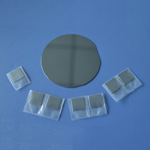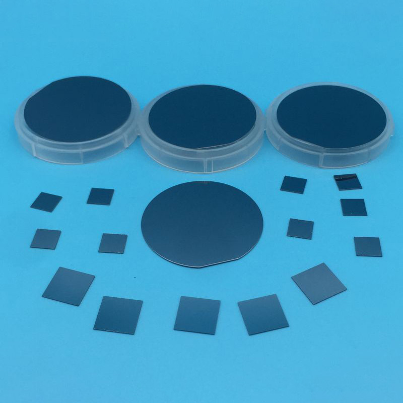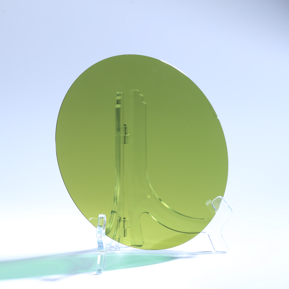
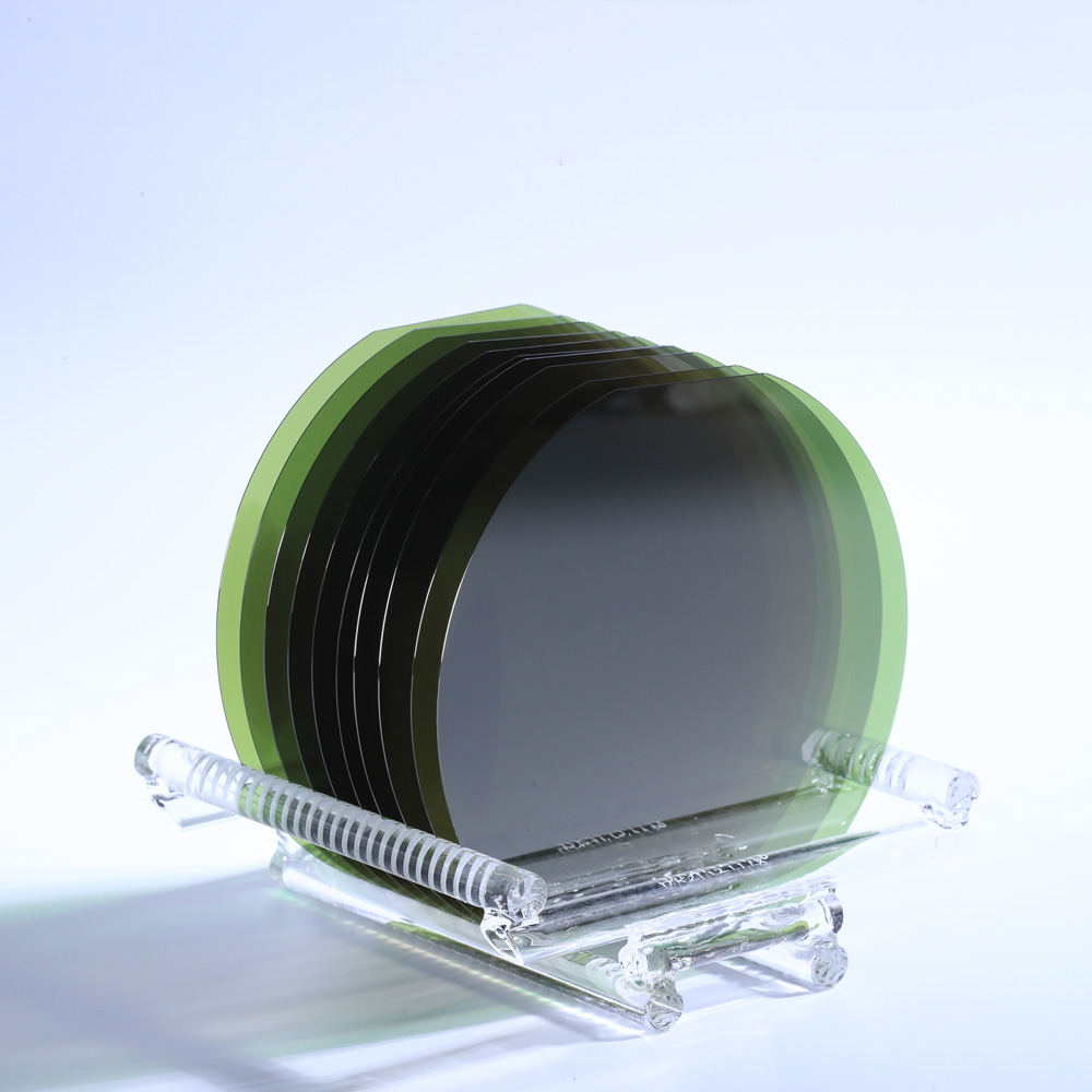
SiC Silicon Carbide Wafers
Compound Semiconductor Wafers

-
+86-17701852595 WhatsApp
-
sales@plutosemitech.com Email
Silicon Carbide wafers are wide-bandgap semiconductor substrate materials based on high-purity silicon carbide single crystals, formed through directional growth, precision cutting, grinding, and ultra-precision polishing. They are primarily used in the manufacturing of devices for high-power, high-voltage, and high-temperature applications. Compared to traditional silicon-based wafers, these wafers exhibit significant differences in core physical properties such as lattice stability, thermal conductivity, and electric field breakdown strength, making them indispensable in high-reliability electronic systems. In terms of defect control, Silicon Carbide wafers utilize high-intensity optical inspection and strict grading standards to manage micropipe density, basal plane dislocations, and screw dislocations, creating a clear distinction between different grades of wafers in terms of cost and performance. This design philosophy, centered on process stability, gives them clear engineering value and a foundation for large-scale manufacturing in the power semiconductor industry.

SiC Silicon Carbide Wafers Specifications
| Diameter | 150±0.5mm, 200±0.25 mm | ||
| Thickness 4H | 350 μm±25μm | ||
| 500 μm±25μm | |||
| Wafer Orientation | Off axis : 4.0° toward 1120 ±0.5° | ||
| Micropipe Density | ≤ 0.2 cm-2 | ≤ 5 cm-2 | ≤ 10 cm-2 |
| BPD | ≤ 1500ea/cm2 | ≤ 2000ea/cm2 | NA |
| TSD | ≤ 300ea/cm2 | ≤ 1000ea/cm2 | NA |
| Resistivity | 0.015~0.025 Ω·cm | ||
| Edge exclusion | 3 mm | ||
| TTV/Bow /Warp | ≤ 3μm / ≤ 5μm / ≤ 10μm | ||
| Roughness | Polish Ra ≤ 0.2 nm | ||
| Cracks by high intensity light | None | None | 1 allowed, ≤ 1 mm |
| Hex Plates by high intensity light | Cumulative area≤ 1 % | Cumulative area≤ 1 % | Cumulative area≤ 3 % |
| Polytype Areas by high intensity light | None | Cumulative area≤ 2 % | Cumulative area≤ 5% |
| Scratches by | 3 scratches to 1× | 5 scratches to 1× | 8 scratches to 1× |
| high intensity light | wafer diameter | wafer diameter | wafer diameter |
| cumulative length | cumulative length | cumulative length | |
| Edge chip | None | 3 allowed, ≤ 0.5 mm each | 5 allowed, ≤ 1 mm each |
| Contamination by | None | ||
| high intensity light | |||
| OEM/ODM | Accept | ||
| Compay Nature | China Manufacturers Suppliers Factory | ||
SiC Silicon Carbide Wafers Features
1. Crystalline Stability
The Silicon Carbide Wafer utilizes a 4H crystal structure with a band gap of approximately 3.26 eV, maintaining a stable band structure under high electric field conditions. Through a 4.0° off-axis design towards the 1120 direction, the risk of step bunching is effectively reduced, ensuring that the epitaxial layer thickness uniformity deviation is controlled within the process-allowed range. In actual testing, the cumulative area of polycrystalline regions is limited to within 2%, and high-grade wafers can achieve a polycrystalline-free distribution, guaranteeing device consistency and electrical parameter stability at the crystal structure level.
2. Controllable Defects
This Silicon Carbide Wafer features graded control of micropipe density, with the highest grade achieving a level of ≤0.2 cm⁻². Basal plane dislocation density and screw dislocation density are controlled within the ranges of ≤1500 ea/cm² and ≤300 ea/cm², respectively, significantly reducing leakage current and early failure probability. Through high-intensity optical inspection, cracks, hexagonal flakes, and polymorphic regions are screened on a wafer-by-wafer basis, ensuring predictable defect distribution in wafers entering the process and improving overall yield controllability.
3. Uniform Resistivity
The bulk resistivity of the Silicon Carbide Wafer is stably controlled within the range of 0.015~0.025 Ω·cm, and through radial uniformity adjustment, the resistivity deviation is maintained within a narrow range. This stability is particularly crucial for high-current density devices, reducing localized heating and current crowding. In power device manufacturing, uniform resistivity distribution helps achieve consistent threshold voltage and conduction characteristics, reducing the risk of device parameter variation at the material level.
4. Morphological Precision
This Silicon Carbide Wafer strictly controls geometric precision with TTV ≤3 μm, Bow ≤5 μm, and Warp ≤10 μm, making it compatible with mainstream automated transfer and photolithography focusing systems. The edge exclusion zone is set at 3 mm, balancing process window and material utilization. High morphological stability effectively reduces bonding defects and focusing errors, providing a reliable foundation for subsequent multi-layer processes and avoiding yield losses due to warping.
5. Surface Quality
The wafer's polished surface roughness is Ra ≤0.2 nm, meeting the interface cleanliness requirements for high-quality epitaxial growth. Under high-intensity optical inspection, the highest-grade products show no cracks or edge chipping, significantly reducing process risks caused by hidden defects. With strict control over scratches and edge defects, this Silicon Carbide wafer is suitable for high-yield, high-repeatability mass production environments.
SiC Silicon Carbide Wafers Process Flow
1. Raw material preparation:
The production of SiC Silicon Carbide Wafer begins with the selection of high-purity silicon powder and carbon source (such as graphite). These raw materials need to undergo rigorous purification to remove any impurities that may affect the quality of the crystal. Only raw materials with a purity of 99.999% can enter the subsequent production process.
2. Crystal growth:
The crystal growth of SiC Wafer usually adopts physical vapor transport (PVT), which is a mature crystal growth technology. During the PVT process, silicon powder and carbon source are heated to high temperatures (about 2000°C to 2500°C) to form a gas phase reaction, and finally deposited on the seed crystal to form a SiC single crystal. The entire growth process needs to be carried out in a vacuum or inert gas environment to avoid external contamination.
3. Temperature and pressure control:
During the crystal growth process, precise control of temperature and pressure is crucial. Plutosemi uses advanced temperature control systems and pressure regulators to ensure that the temperature and pressure in the reactor are always kept at the optimal state, thereby generating high-quality SiC crystals.
4. Crystal cutting and grinding:
After the crystal growth is completed, the original SiC ingot will be cut into thin wafers. Plutosemi uses high-precision cutting equipment to ensure that the thickness of the wafer is uniform (the error is controlled within ±25 μm). The cut wafer also needs to go through multiple grinding processes to achieve the surface flatness and roughness requirements.
5. Polishing and cleaning:
Polishing is a key step in SiC wafer production, aiming to further improve the surface quality of the wafer. Plutosemi uses chemical mechanical polishing (CMP) technology to control the surface roughness of the wafer to Ra ≤ 0.2 nm. After polishing, the wafer also needs to go through a rigorous cleaning process to remove residual particles and contaminants.
6. Quality inspection:
Each SiC wafer needs to undergo multiple quality inspections before leaving the factory, including micropipe density detection, surface defect analysis, resistivity measurement, and optical performance evaluation. Plutosemi uses advanced testing equipment such as scanning electron microscopes (SEM) and atomic force microscopes (AFM) to ensure that wafers meet strict industry standards.
7. Packaging and transportation:
In order to prevent wafers from being damaged during transportation, Plutosemi uses professional anti-static and shockproof packaging solutions. Wafers are placed in a dedicated protective box and fixed with cushioning materials to ensure that they remain intact during transportation.
SiC Silicon Carbide Wafers Application
1. Power Devices
Silicon Carbide wafers are widely used as substrates for high-voltage power devices. Their high breakdown field strength allows devices to operate stably at voltage levels of 1200 V and above. Compared to traditional materials, this allows for a reduction in the thickness of the drift layer under the same voltage conditions, thereby reducing conduction losses. In power modules, this characteristic helps achieve higher efficiency and smaller size designs, meeting the needs of high-density integration.
2. New Energy Systems
In new energy conversion systems, Silicon Carbide wafers support high-frequency and high-temperature operating environments, allowing the system switching frequency to be increased to tens of kHz or more, significantly reducing the size of magnetic components. This material characteristic directly promotes improved system efficiency and reduces overall thermal management pressure, which is of practical value for energy conversion stability.
3. Industrial Power Supplies
Industrial-grade power supply equipment requires extremely high long-term stability. Silicon Carbide wafers maintain stable electrical performance even at high temperatures, reducing parameter drift caused by temperature increases. In continuous operation scenarios, these wafers help extend system maintenance cycles and improve overall equipment availability.
4. Rail Transit
Rail transit traction systems have extremely high requirements for the voltage resistance and reliability of power devices. Silicon Carbide wafers support high voltage and fast response characteristics, enabling more compact power conversion unit designs. By reducing system energy loss, this material helps improve overall operating efficiency and reduce the burden on the cooling system.
5. High-End Manufacturing
In the field of high-end equipment manufacturing, Silicon Carbide wafers support high-precision and high-stability power control needs, meeting the strict requirements for device consistency in complex control systems.
Its predictable material properties provide a stable foundation for high-reliability system design, reducing long-term operating risks.
SiC Silicon Carbide Wafers FAQ
Q: What are the core differences between Silicon Carbide Wafers and silicon wafers?
A: Silicon Carbide Wafers have a wider band gap and higher breakdown electric field strength, allowing them to maintain stable operation in high-voltage and high-temperature environments. This significantly reduces energy loss and alleviates system heat dissipation pressure in high-power applications.
Q: How to choose between different wafer grades?
A: The main differences between different grades lie in the control standards for micropipe density and dislocation count. High-grade wafers are suitable for applications requiring extremely high reliability, while standard-grade wafers offer a balance between performance and cost. The specific choice depends on the device design objectives.
Q: What is the impact of off-axis angle on the manufacturing process?
A: The 4.0° off-axis design helps suppress surface step bunching and improves the uniformity of epitaxial layer growth. This is especially important for multi-layer devices, reducing the impact of interface defects on electrical performance.
Q: Does wafer warpage affect mass production?
A: The warpage index is strictly controlled within ≤10 μm, making it compatible with mainstream automated equipment. Stable geometric morphology helps reduce anomalies during transfer and photolithography processes, improving overall process stability.
Q: Do you support OEM or ODM?
A: Silicon Carbide Wafers support OEM and ODM cooperation models and can be customized according to parameters such as diameter, thickness, and defect level to meet the comprehensive needs of different projects in terms of performance and cost.
Packaging and Transportation
The packaging should be able to withstand the impact, vibration, stacking and extrusion that may be encountered during transportation, while also it has to easy to load, unload and handle.
We use professional wafer box packaging. The wafer box is protected by a double layer bag, the inside is a PE bag that can be dust-proof, and the outside is a aluminum foil bag that can be isolated from the air. The two-layer bags are vacuum-packed.
We will choose carton models according to different sizes of products. And between the product and the carton filled with shock-proof EPE foam, play a comprehensive protection.
Finally choose air transport to reach the customer's hands. This allows customers in any country and region to receive the product in the fastest time.
We comply with the Material Safety Data Sheet (MSDS) rules to ensure that the products transported are free of harmful substances and will not cause environmental pollution and explosion and other possible hazards.

Enterprise Strength
Factory Area: 3000 sq
Process:
1. Shaping→2. Edge Profile→3. Lapping→4. Polishing→5. Cleaning→6. Packing→7. Transportation
Capacity:
Glass Wafer --- 30K pcs
Silicon Wafer --- 20K pcs
(Equal to 6in)

Quality Assurance
Quality inspection method: Product inspection in accordance with SEMI standard or according to customer's requirements, together with product COA.
Warranty period: In accordance with the contract requirements.
Quality system management:
●Organize production according to ISO9001 and other quality system standards.
Quality management system and measures:
●Establish a strict quality assurance system, the heads of all departments and quality engineers to ensure the coordinated operation of the quality system.
●Strengthen the quality inspection system, strengthen the process quality control
●Strict material quality control, ensure that the input materials meet the design requirements and technical specifications.
●Implement a timely filing system for technical data to ensure that all processing technical data is complete/accurate.
Quality control in the production stage:
●Production preparation stage: carefully organize relevant personnel to learn product drawings and technical rules, and improve the technical level of employees.
●Quality control of the production process: the implementation of a strict handover system, the previous step of the process to the next step of the transfer, should be detailed processing. At the same time, strengthen the quality inspection system to ensure the quality of each step of the process.
●Quality acceptance: All processes must be quality acceptance before proceeding to the next process.

Pre-sales and After-sales
Pre-sales Service
Professional technical support and commercial team to help you determine product specifications according to product use, and issue specifications.
On-purchase Service
Produce products according to the confirmed specifications and our process.
After Sale Service
We will respond to any product problems encountered by customers or process problems encountered by customers within 24 hours. We can choose from various forms of service, such as email, video conference and so on.
Plutosemi Co., Ltd. was established in 2019, headquartered in Nanhai, Foshan, focusing on the research and development, production, and sales of high-performance semiconductor materials.
Advanced production capacity: We have three major production bases in China, with a monthly production capacity of 100000 equivalent 6-inch silicon wafers and 30000 equivalent 8-inch glass wafers, ensuring stable and efficient product supply for our customers.
High quality products: We provide efficient and stable product supply innovative solutions in the fields of glass wafers, silicon polishing wafers, epitaxial wafers (EPI), silicon on insulator wafers (SOI), and more. Our silicon wafers have the characteristics of ultra-thin, ultraflat, and high-precision, which can meet the needs of various high-end applications. Our glass and quartz substrates are also renowned for their high smoothness and precise aperture design.