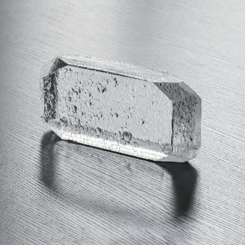
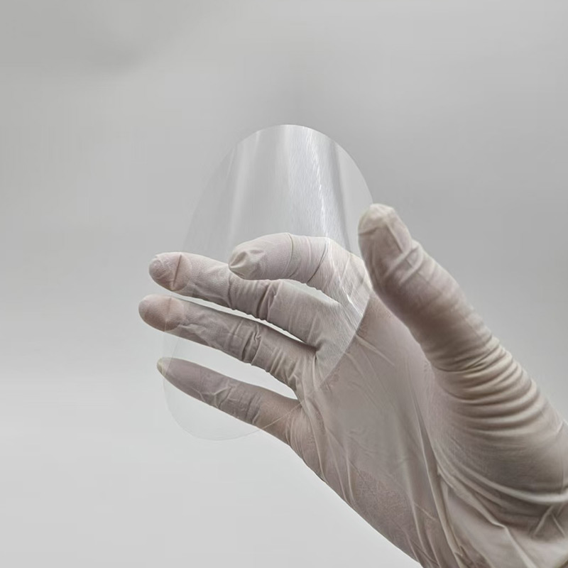

Corning 7980 Glass Wafer
Glass Wafer

-
+86-17701852595 WhatsApp
-
sales@plutosemitech.com Email
Corning 7980 Glass Wafer is a high-quality glass wafer, which is based on SiO₂ and produced using advanced manufacturing processes. This wafer plays an important role in the field of semiconductor manufacturing and is an indispensable key material in the production process of many high-tech products. Its unique material and structure enable it to meet strict industrial standards, provide a reliable carrier for various precision microelectronics processing, and is one of the important supporting materials for the development of modern electronic technology.

Corning 7980 Glass Wafer Specifications
| Thermal property | |
| Item | Value |
| Thermal Expansion α(-100 C to +200 C) | 0.48 x 10⁻⁶(ppm/C) |
| Specific Heat Capacity Cp(20 - 100 °C) | 0.770 J/(g·K) |
| Thermal Conductivity | 1.38 W/(m·K) |
| Mechanical property | |
| Item | Value |
| Density ρ (25 °C) | 2.20 g/cm3 |
| ShearModulus G | 31 GPa |
| Poisson's ratio | 0.16 |
| Knoop Hardness(100g load) | 552 kg/mm2 |
| Tensile Strength | 54 MPa |
| Technical Specifications | |||||||
| Diameter | 2inch | 3inch | 4inch | 5inch | 6inch | 8inch | 12inch |
| Thickness (um) | Depends on Request | ||||||
| Material | 7980 | ||||||
| Grade/Brand | Corning | ||||||
| Surface Finished | DSP、SSP、DSL | ||||||
| TTV (um) | <5 | <5 | <5 | <5 | <5 | <10 | <15 |
| Bow/Warp (um) | <20 | <20 | <30 | <30 | <30 | <40 | <60 |
| Ra (nm) | <1 | ||||||
| S/D (um) | 40/20 | ||||||
Corning 7980 Glass Wafer Features
Excellent optical performance
Corning 7980 Glass Wafer has excellent optical performance and extremely high transparency. Its transmittance in visible light and some ultraviolet light bands can reach more than 90%, which makes it perform well in the manufacture of optoelectronic devices. For example, in the field of optical communications, it can ensure the efficient transmission of optical signals, reduce signal attenuation, and provide strong support for the construction of high-speed and stable optical communication networks. At the same time, its refractive index is stable, with a very small fluctuation range of only ±0.001, which accurately controls the propagation path of light and meets the needs of high-precision optical processing and detection.
Super strong chemical stability
In terms of chemical stability, Corning 7980 Glass Wafer performs well. It can resist the erosion of a variety of strong acids, strong alkalis and organic solvents. Even under extreme conditions of long-term contact with high-concentration hydrofluoric acid (HF) solution (concentration up to 49%), its surface corrosion rate is only 0.01 mm/year, which is much lower than the 0.1 mm/year specified by the industry standard. It can maintain stable physical and chemical properties to ensure that the surface of the chip is not affected by chemical reactions.
High dimensional accuracy
Corning 7980 Glass Wafer has extremely high dimensional accuracy, which can meet the requirements of semiconductor manufacturing for micron-level or even nanometer-level accuracy. Its diameter tolerance is controlled within ±0.05 mm, and its thickness tolerance is only ±0.01 mm, which is at the leading level in the industry. Taking an 8-inch wafer as an example, its diameter error range is only 0.05 mm, which means that in large-scale integrated circuit manufacturing, high-density chip layout can be achieved, improving the integration and performance of the chip.
Excellent flatness
The flatness of the wafer is very excellent, and its surface flatness can reach the standard of 1/10λ (helium-neon laser with a wavelength of 632.8 nm), which is equivalent to a surface height difference of only 0.063 μm. In the lithography process of semiconductor manufacturing, the lithography machine needs to accurately project the lithography pattern on the surface of the wafer. Any tiny surface unevenness may cause pattern distortion and affect the performance of the chip. The high flatness of Corning 7980 Glass Wafer can ensure uniform coating of the photoresist layer and clear and accurate transfer of the photolithography pattern to the wafer surface, thereby ensuring the micro-nanostructure processing accuracy of semiconductor devices.
Good thermal stability
Corning 7980 Glass Wafer has good thermal stability, and its thermal expansion coefficient is as low as 0.5 ppm/°C (parts per million per degree Celsius), which is much lower than the 9 ppm/°C of ordinary glass materials. In the semiconductor manufacturing process, from low-temperature epitaxial growth to high-temperature diffusion, annealing and other process links, the temperature variation range may be from -50°C to 1200°C. This low thermal expansion coefficient makes the size of the wafer change very little when the temperature changes, and can maintain stable physical and chemical properties, avoid problems such as wafer deformation and cracking caused by thermal stress, and ensure the manufacturing quality and performance stability of semiconductor devices.
High mechanical strength
In terms of mechanical strength, Corning 7980 Glass Wafer performs well, and its bending strength can reach 200 MPa, which is more than 3 times that of ordinary glass. During semiconductor manufacturing and transportation, the wafer can withstand greater mechanical stress without being easily damaged. Good mechanical strength also helps to improve the stability of the wafer in a complex process environment, ensure the smooth progress of the semiconductor manufacturing process, reduce the risk of production interruption caused by wafer damage, and improve production efficiency.
Environmentally friendly and pollution-free
Corning 7980 Glass Wafer strictly follows environmental protection standards and does not use any harmful substances, such as heavy metals such as lead, mercury, and cadmium, in the production process, and complies with the requirements of the RoHS (Restriction of the Use of Certain Hazardous Substances) Directive. This not only helps to protect the environment and reduce pollution to the ecosystem, but also meets the environmental protection requirements of the modern electronics manufacturing industry.
Perfect customized service
Corning 7980 Glass Wafer provides perfect customized services and can be customized according to the special needs of customers. In addition to the standard 2, 4, 6, 8, and 12-inch wafer sizes, non-standard wafers can also be customized according to the specific requirements of customers, ranging from 1 inch to 30 inches. At the same time, the surface treatment and doping concentration of the wafer can also be customized according to customer needs to meet the needs of different customers in different application fields.
Corning 7980 Glass Wafer Process Flow
1. Preparation of basic materials
The basic material of Corning 7980 Glass Wafer is high-purity silicon dioxide (SiO₂). First, high-quality quartz sand is selected as the raw material, and impurities are removed through high-temperature smelting to ensure that the purity of SiO₂ reaches more than 99.99%. This process is carried out in a dedicated high-temperature furnace, and the temperature is controlled at around 2000°C to ensure that the quartz sand is completely melted and forms a uniform glass melt. During the smelting process, the atmosphere and temperature are strictly controlled to prevent the mixing of impurities, providing a pure raw material basis for subsequent wafer growth.
2. Composite growth method
Corning 7980 Glass Wafer is manufactured using the composite growth method. This method combines a variety of advanced growth technologies, such as the Czochralski method and the zone refining method. In the Czochralski method, the molten SiO₂ solution is slowly pulled into a wafer through a seed crystal, and the structural integrity of the wafer is ensured by precisely controlling the crystal pulling speed and temperature gradient. The zone melting method is used to further improve the purity of the material. By slowly moving the heating area, impurities are enriched at one end, thereby obtaining a high-purity wafer. The combination of the composite growth method makes Corning 7980 Glass Wafer reach high standards in both structure and performance.
3. Class 100 clean room production
The production process of Corning 7980 Glass Wafer is carried out in a Class 100 clean room with a cleanliness level that meets ISO Class 5 standards. The air in the clean room is efficiently filtered, and the number of particles with a diameter greater than 0.5 microns per cubic meter of air does not exceed 100. This high-cleanliness environment can effectively prevent particulate contamination and ensure the purity and quality of the wafer surface. In the clean room, all production equipment and operators are strictly cleaned and disinfected to avoid any possible sources of contamination and ensure the high quality standards of the wafer during the production process.
4. Precision processing and testing
After production, Corning 7980 Glass Wafer undergoes a series of precision processing and testing processes. First, the wafer is surface treated using high-precision grinding and polishing equipment to ensure that its surface flatness reaches the standard of 1/10λ. Then, the surface flatness, dimensional accuracy and chemical stability of the wafer are strictly tested by advanced testing equipment such as optical interferometers and atomic force microscopes (AFM). During the testing process, any wafers that do not meet the standards will be screened out to ensure that every wafer delivered to customers meets high quality standards.
5. Customized processing
In order to meet the specific needs of customers, Corning 7980 Glass Wafer provides customized processing services. According to customer requirements, special coatings such as anti-reflective coatings, conductive coatings, etc. can be applied to the surface of the wafer. At the same time, doping treatment can also be performed according to customer needs to adjust the electrical properties of the wafer. These customized processing processes are carried out in a dedicated process workshop, strictly following the customer's specifications to ensure the high quality and high performance of customized products.
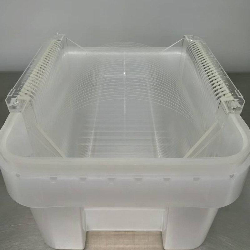
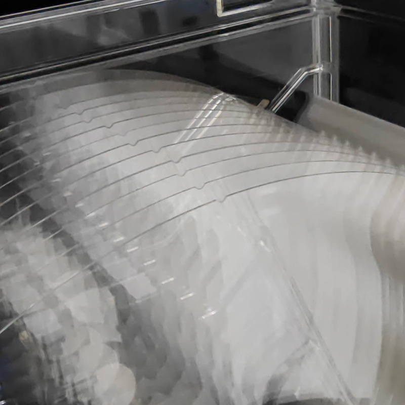
6. Packaging and transportation
Corning 7980 Glass Wafer also strictly follows industry standards during packaging and transportation. The wafer is placed in a dedicated anti-static and shockproof packaging box to ensure that it is not damaged during transportation. The interior of the packaging box is made of high-purity polyethylene foam material, which can effectively absorb vibration and impact. During transportation, professional logistics services are used to ensure that the wafers can be delivered to customers safely and on time. At the same time, the company also provides logistics tracking services to facilitate customers to understand the product transportation status at any time.
7. Quality Control and Certification
The production process of Corning 7980 Glass Wafer strictly follows the ISO 9001 quality management system standard to ensure the stability and consistency of product quality. The company regularly conducts internal quality audits and external certification audits to ensure that the production process meets international standards. The product has also passed RoHS certification to ensure its environmental protection and safety. Through a strict quality control and certification system, Corning 7980 Glass Wafer provides customers with high-quality and high-reliability products to meet the needs of different application fields.
Corning 7980 Glass Wafer Application
MEMS and Electronics
MEMS and electronics use glass wafers for fabrication in wafer packaging and substrate carriers. In MEMS and electronics applications, glass wafers are used in wafer packaging of sensitive components because of their superior functionality and extreme reliability over time and in the face of harsh environments. As a carrier substrate, glass is selected because of its thermal stability and chemical resistance. In the medical device industry, these wafers are used to promote airtight MEMS enclosures
Semiconductors
Glass wafers are used as carrier substrates in the production of semiconductor wafers, which are made of finer materials that are easily bent or torn. Glass substrate components can safely handle semiconductor wafers, despite their fine and thin texture. Glass was chosen because of its superior chemical and thermal stability, and the potential for reuse to reduce the cost and environmental impact of some applications.
Biotechnology
Glass wafers are used in a variety glass substrate of biotechnology applications. Borosilicate glass is a premium choice in medical device glass because of its excellent resistance to high temperature and energy as well as radiation exposure, for example in X-ray equipment. Wafers are also used to produce microfluidic chips by using nanoimprint lithography, in which glass acts as the substrate. Glass provides the clear optical transparency required for many biotechnology applications, making it a common choice for use as overlays on devices of silicon. Wafer bonding processes, such as anode bonding and thermal bonding, create air-tight sealing.
Integrated Circuit
Glass wafers are used in a variety of integrated circuit (IC) packaging applications, providing better performance and cost effectiveness as substrates. Glass through-holes (TGVS) and wafer-grade glass caps (WLC) are improved packaging solutions that offer enhanced technical performance, this is thanks to specific glass characteristics, including stiffness and roughness below 0.5 nm rms. Glass protects the IC from shock and corrosion while maintaining the pins and leads that connect to the external circuit.
Packaging and Transportation
The packaging should be able to withstand the impact, vibration, stacking and extrusion that may be encountered during transportation, while also it has to easy to load, unload and handle.
We use professional wafer box packaging. The wafer box is protected by a double layer bag, the inside is a PE bag that can be dust-proof, and the outside is a aluminum foil bag that can be isolated from the air. The two-layer bags are vacuum-packed.
We will choose carton models according to different sizes of products. And between the product and the carton filled with shock-proof EPE foam, play a comprehensive protection.
Finally choose air transport to reach the customer's hands. This allows customers in any country and region to receive the product in the fastest time.
We comply with the Material Safety Data Sheet (MSDS) rules to ensure that the products transported are free of harmful substances and will not cause environmental pollution and explosion and other possible hazards.

Enterprise Strength
Factory Area: 3000 sq
Process:
1. Shaping→2. Edge Profile→3. Lapping→4. Polishing→5. Cleaning→6. Packing→7. Transportation
Capacity:
Glass Wafer --- 30K pcs
Silicon Wafer --- 20K pcs
(Equal to 6in)

Quality Assurance
Quality inspection method: Product inspection in accordance with SEMI standard or according to customer's requirements, together with product COA.
Warranty period: In accordance with the contract requirements.
Quality system management:
●Organize production according to ISO9001 and other quality system standards.
Quality management system and measures:
●Establish a strict quality assurance system, the heads of all departments and quality engineers to ensure the coordinated operation of the quality system.
●Strengthen the quality inspection system, strengthen the process quality control
●Strict material quality control, ensure that the input materials meet the design requirements and technical specifications.
●Implement a timely filing system for technical data to ensure that all processing technical data is complete/accurate.
Quality control in the production stage:
●Production preparation stage: carefully organize relevant personnel to learn product drawings and technical rules, and improve the technical level of employees.
●Quality control of the production process: the implementation of a strict handover system, the previous step of the process to the next step of the transfer, should be detailed processing. At the same time, strengthen the quality inspection system to ensure the quality of each step of the process.
●Quality acceptance: All processes must be quality acceptance before proceeding to the next process.

Pre-sales and After-sales
Pre-sales Service
Professional technical support and commercial team to help you determine product specifications according to product use, and issue specifications.
On-purchase Service
Produce products according to the confirmed specifications and our process.
After Sale Service
We will respond to any product problems encountered by customers or process problems encountered by customers within 24 hours. We can choose from various forms of service, such as email, video conference and so on.
Plutosemi Co., Ltd. was established in 2019, headquartered in Nanhai, Foshan, focusing on the research and development, production, and sales of high-performance semiconductor materials.
Advanced production capacity: We have three major production bases in China, with a monthly production capacity of 100000 equivalent 6-inch silicon wafers and 30000 equivalent 8-inch glass wafers, ensuring stable and efficient product supply for our customers.
High quality products: We provide efficient and stable product supply innovative solutions in the fields of glass wafers, silicon polishing wafers, epitaxial wafers (EPI), silicon on insulator wafers (SOI), and more. Our silicon wafers have the characteristics of ultra-thin, ultraflat, and high-precision, which can meet the needs of various high-end applications. Our glass and quartz substrates are also renowned for their high smoothness and precise aperture design.