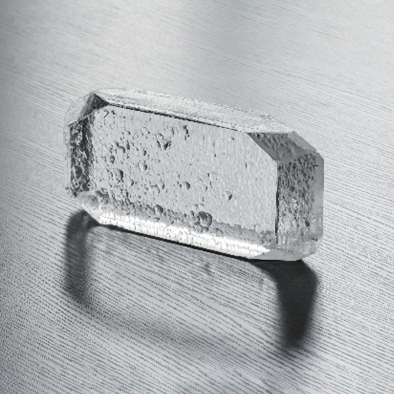

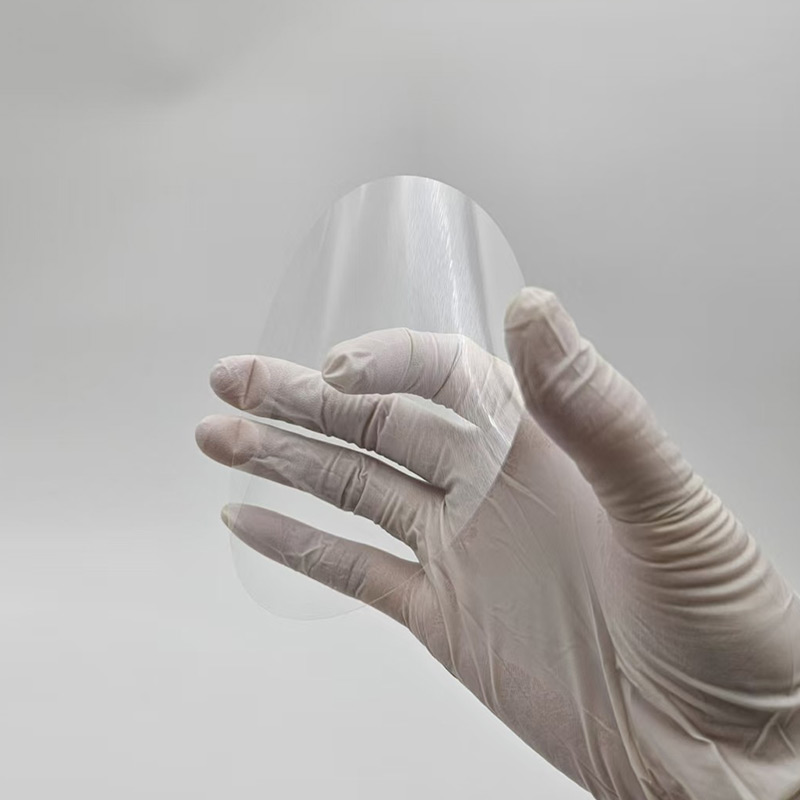

Corning Eagle XG Glass Wafer
Glass Wafer

-
+86-17701852595 WhatsApp
-
sales@plutosemitech.com Email
Corning Eagle XG Glass Wafer is a high-quality glass wafer produced. It is made of silicon dioxide (SiO₂) as the base material and is manufactured using a composite growth method. This wafer has a wide range of sizes, from 2 inches to 12 inches, and can even be customized according to customer needs, to meet the diverse needs of wafer sizes in different industries and application scenarios. It strictly follows environmental protection standards during the production process, complies with the requirements of the RoHS directive, and provides customers with environmentally friendly and reliable material options. In terms of logistics and distribution, logistics express delivery is used to ensure that the products can be delivered quickly and safely to customers around the world, especially in overseas markets with good market coverage. Its unique material properties and production process give it broad application prospects in many fields such as electronics and optics.

Corning Eagle XG Glass Wafer Specifications
| Product Name | Eagle XG Glass Wafer |
| Size | 2/4/6/8/12inch or customized |
| Package | Hundred-class clean room |
| Customized Support | YES |
| RoHS | YES |
| Delivery Methods | Logistics Express |
| Marketable Area | oversea |
| Growth Method | Composite |
| Base | SiO2 |
| Dielectric Constant(k=EO/E) | 5-6 |
| Refractive(@589.3nm) | 1.50-1.52 |
| Mechanical property | |
| Item | Value |
| Density ρ (25 °C) | 2.3-2.5 g/cm3 |
| Poisson's ratio | 0.20-0.25 |
| Vickers hardness HK0.2/25 | 640 |
| Thermal property | |
| Item | Value |
| Thermal Expansion (0 to 300℃) | 3-3.5(ppm/C) |
| Strain Point (°C) | 650-700 |
| Anneal Point | 700-750 |
| Diameter | 2inch | 3inch | 4inch | 5inch | 6inch | 8inch | 12inch |
| Thickness (um) | Depends on Request | ||||||
| Material | Eagle XG | ||||||
| Grade/Brand | Corning | ||||||
| Surface Finished | DSP、SSP、DSL | ||||||
| TTV (um) | <5 | <5 | <5 | <5 | <5 | <10 | <15 |
| Bow/Warp (um) | <20 | <20 | <30 | <30 | <30 | <40 | <60 |
| Ra (nm) | <1 | ||||||
| S/D (um) | 40/20 | ||||||
| special indexes: Ultra-flat glass wafer: TTV<1um Ultra-thin glass wafer: Thickness:0.1-0.3um Ultra-smooth glass wafer: Ra≤0.2nm | |||||||
Corning Eagle XG Glass Wafer Features
Various sizes
Corning Eagle XG Glass Wafer has a standard size series from 2 inches to 12 inches, and also provides customized size services. This wide range of size selection can meet the specific needs of different customers in different application scenarios. Whether it is small electronic equipment manufacturing or large optical system development, you can find the right wafer size, providing customers with great flexibility and convenience.
Clean production environment
This Corning Eagle XG Glass Wafer is produced in a Class 100 clean room. This high-cleanliness production environment can effectively reduce particulate contamination on the surface of the wafer. In semiconductor manufacturing and precision optical applications, particulate contamination may cause product performance degradation or even scrap. Therefore, the production conditions of the Class 100 clean room provide excellent quality assurance for the product, ensuring that the surface quality of the wafer meets high-precision requirements, thereby improving the yield and reliability of the product.
Environmental compliance
Corning Eagle XG Glass Wafer fully complies with the requirements of the RoHS Directive. The RoHS Directive aims to restrict the use of hazardous substances in electronic and electrical products to protect the environment and human health. Choosing this product means that customers can meet increasingly stringent environmental regulations and avoid the risks of using materials that do not meet environmental standards. It also reflects the company's sense of responsibility for environmental protection and helps to enhance the company's social image and market competitiveness.
Excellent insulation performance
It has a dielectric constant of 5-6 (k=EO/E), which indicates that it has good insulation performance. In electronic devices, good insulation performance is essential to prevent current leakage and ensure the normal operation of circuits. This excellent insulation property enables Corning Eagle XG Glass Wafer to play an important role in various electronic and optical applications, providing reliable material support for the stable operation of high-performance electronic devices.
Reliable optical performance
The refractive index of this product is 1.50-1.52 at a wavelength of 589.3 nanometers. This precise refractive index range ensures stable light propagation and precise optical imaging in optical applications. In the design of optical systems, accurate refractive index is a key factor in achieving precise matching of optical components and optimizing system performance. This feature of Corning Eagle XG Glass Wafer enables it to meet the needs of high-precision optical applications, such as high-end optical lenses, optical communication devices, etc., providing a strong material guarantee for technological innovation and development in the field of optics.
Corning Eagle XG Glass Wafer Process Flow
Selection of basic materials
Corning Eagle XG Glass Wafer uses silicon dioxide (SiO₂) as its basic material. Silicon dioxide is a basic material widely used in the fields of electronics and optics, with good insulation, optical and chemical stability. When selecting basic materials, the purity and quality of silicon dioxide are strictly controlled to ensure that it can meet the high standards of product performance and quality. By carefully screening and processing basic materials, a solid foundation is laid for the subsequent wafer manufacturing process, ensuring the excellent performance of the final product.
Composite growth method
Corning Eagle XG Glass Wafer is manufactured using a composite growth method. This growth method combines a variety of advanced growth technologies to gradually grow silicon dioxide materials into wafers with specific sizes and performance under precisely controlled conditions. The composite growth method can effectively improve the growth rate and quality stability of wafers, and can also achieve fine control of the internal structure and performance of wafers. By optimizing composite growth process parameters such as growth temperature and growth rate, it can ensure that the wafers reach the industry-leading level in terms of dimensional accuracy, surface quality, optical performance, etc., and meet the strict requirements of wafer performance in different application scenarios.
Precision machining and molding
After the wafer growth is completed, precision machining and molding processes are required. First, the wafer is cut and processed into the required size and shape. PLUTOSEMI uses advanced cutting technology and equipment to achieve high-precision wafer cutting, ensuring that the size accuracy of the cut wafer reaches the micron level. Then, the cut wafer is ground and polished to improve the surface quality and optical performance of the wafer. Through the precision grinding and polishing process, the tiny defects and unevenness on the wafer surface can be removed, so that the wafer surface can reach mirror-level smoothness, thereby improving its performance in optical applications and meeting the requirements of high-precision optical component manufacturing.
Surface treatment and optimization
In order to further improve the performance and application value of Corning Eagle XG Glass Wafer, it is also necessary to perform surface treatment and optimization. PLUTOSEMI uses a variety of surface treatment technologies, such as chemical vapor deposition (CVD), physical vapor deposition (PVD), etc., to deposit one or more layers of specific thin film materials on the surface of the wafer. These thin film materials can give wafers special properties according to different application requirements, such as improving their anti-reflection properties, increasing their surface hardness, and improving their chemical stability. By precisely controlling the surface treatment process parameters, the surface performance of the wafer can be precisely regulated, so that it can better meet the requirements of various complex application environments and enhance the market competitiveness of the product.
Quality Inspection and Control
Throughout the production process, PLUTOSEMI has established a strict quality inspection and control system. From the procurement of basic materials, monitoring of the composite growth process, to the final inspection after the wafer is processed and formed, every link is subject to strict quality inspection and control. Advanced inspection equipment and technology, such as optical inspection systems and electron microscopes, are used to comprehensively inspect the dimensional accuracy, surface quality, optical properties, electrical properties and other indicators of the wafer. Only wafers whose indicators meet industry standards and product design requirements will be recognized as qualified products and shipped. Through strict quality inspection and control, the product quality of Corning Eagle XG Glass Wafer is ensured to be stable and reliable, providing customers with high-quality product guarantees.
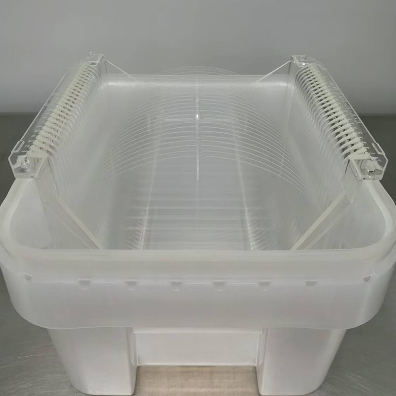
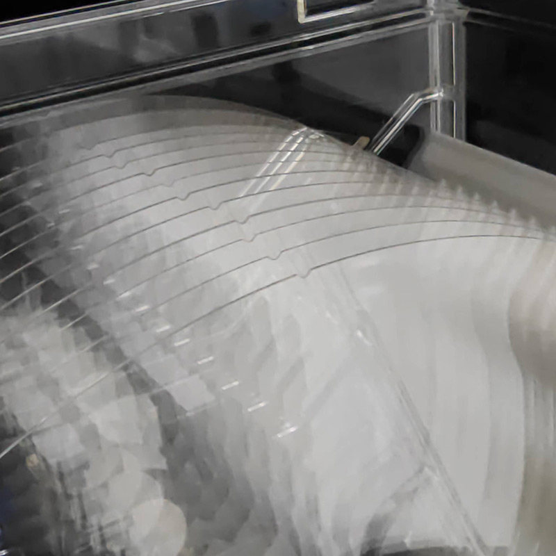
Packaging and Logistics
After the wafer is produced, PLUTOSEMI uses professional packaging technology to package it. According to the characteristics of the product and customer needs, we select appropriate packaging materials and packaging methods to ensure that the wafers are not damaged during transportation. The packaged wafers are placed in a Class 100 clean room environment for storage and shipment preparation to ensure that their surface cleanliness is not contaminated. In terms of logistics and distribution, PLUTOSEMI cooperates with professional logistics companies to use logistics express to deliver products quickly and safely to customers around the world. During the logistics process, we strictly monitor the transportation conditions to ensure that the wafers are not affected by environmental factors such as temperature and humidity during transportation, and to ensure that the products still maintain good quality and performance when they reach the hands of customers.
Corning Eagle XG Glass Wafer Application
Semiconductor Manufacturing
Corning Eagle XG Glass Wafer has important applications in the field of semiconductor manufacturing. It can be used as a substrate material in the process of semiconductor chip manufacturing to grow various semiconductor films. Its good insulation performance and surface quality help improve the performance and reliability of semiconductor devices. In key processes such as lithography and etching, the dimensional accuracy and surface cleanliness of the wafer play a decisive role in the quality of the final product, and the diverse size selection and Class 100 clean room production environment of this wafer can meet these requirements, providing high-quality basic material support for the development of the semiconductor industry.
Optical Component Manufacturing
In terms of optical component manufacturing, Corning Eagle XG Glass Wafer is an ideal choice for manufacturing various optical lenses, prisms, filters and other optical components. Its precise refractive index and good optical performance can ensure that optical components achieve precise light propagation and imaging effects in various optical systems. Whether it is used for camera lenses, microscope lenses or optical components in optical communication devices, this wafer can provide stable and reliable optical performance, meet the strict requirements of different optical applications for materials, and promote the continuous advancement of optical component manufacturing technology.
Display Technology Field
Corning Eagle XG Glass Wafer is also widely used in display technology. With the continuous development of display technology, such as liquid crystal display (LCD), organic light-emitting diode display (OLED), etc., the requirements for substrate materials are getting higher and higher. The size diversity and good surface quality of this wafer enable it to meet the manufacturing needs of display panels of different sizes. Its insulation and optical properties also help to improve the performance and stability of display panels, provide strong material support for the innovation and development of display technology, and promote the development of display technology towards higher resolution, higher contrast and lower power consumption.
Optical communication field
In the field of optical communication, Corning Eagle XG Glass Wafer can be used to manufacture key components in optical communication devices, such as optical waveguides, optical couplers, etc. Its precise refractive index and good optical properties can ensure the efficient transmission and precise coupling of optical signals in optical communication systems. With the continuous development of optical communication technology, the performance requirements for optical communication devices are also getting higher and higher. The excellent characteristics of this wafer enable it to meet the strict requirements for materials in the field of optical communication, provide high-quality material guarantees for the rapid development of optical communication technology, and help achieve faster and more stable optical communication networks.
Biomedical engineering
Corning Eagle XG Glass Wafer also has potential application value in the field of biomedical engineering. For example, in the manufacture of biosensors, it can be used as a sensor substrate material for fixing biomolecules and detecting biosignals. Its good insulation properties and surface quality help improve the sensitivity and stability of biosensors. In addition, in the field of biomedical imaging, such as fluorescence microscopy, its optical properties can also meet the requirements of high-precision imaging, providing reliable material support for research and application in the field of biomedical engineering, and promoting the continuous innovation and development of biomedical technology.
New energy field
In the field of new energy, Corning Eagle XG Glass Wafer can be used to manufacture new energy devices such as solar cells. Its good insulation and optical properties can improve the photoelectric conversion efficiency and stability of solar cells. In the manufacturing process of solar cells, the dimensional accuracy and surface quality of the wafer play a key role in the performance and reliability of the battery, and the diverse size options and Class 100 clean room production environment of this wafer can meet these requirements, providing high-quality basic material support for the development of the new energy industry, and helping to achieve more efficient and environmentally friendly energy utilization methods.
Packaging and Transportation
The packaging should be able to withstand the impact, vibration, stacking and extrusion that may be encountered during transportation, while also it has to easy to load, unload and handle.
We use professional wafer box packaging. The wafer box is protected by a double layer bag, the inside is a PE bag that can be dust-proof, and the outside is a aluminum foil bag that can be isolated from the air. The two-layer bags are vacuum-packed.
We will choose carton models according to different sizes of products. And between the product and the carton filled with shock-proof EPE foam, play a comprehensive protection.
Finally choose air transport to reach the customer's hands. This allows customers in any country and region to receive the product in the fastest time.
We comply with the Material Safety Data Sheet (MSDS) rules to ensure that the products transported are free of harmful substances and will not cause environmental pollution and explosion and other possible hazards.

Enterprise Strength
Factory Area: 3000 sq
Process:
1. Shaping→2. Edge Profile→3. Lapping→4. Polishing→5. Cleaning→6. Packing→7. Transportation
Capacity:
Glass Wafer --- 30K pcs
Silicon Wafer --- 20K pcs
(Equal to 6in)

Quality Assurance
Quality inspection method: Product inspection in accordance with SEMI standard or according to customer's requirements, together with product COA.
Warranty period: In accordance with the contract requirements.
Quality system management:
●Organize production according to ISO9001 and other quality system standards.
Quality management system and measures:
●Establish a strict quality assurance system, the heads of all departments and quality engineers to ensure the coordinated operation of the quality system.
●Strengthen the quality inspection system, strengthen the process quality control
●Strict material quality control, ensure that the input materials meet the design requirements and technical specifications.
●Implement a timely filing system for technical data to ensure that all processing technical data is complete/accurate.
Quality control in the production stage:
●Production preparation stage: carefully organize relevant personnel to learn product drawings and technical rules, and improve the technical level of employees.
●Quality control of the production process: the implementation of a strict handover system, the previous step of the process to the next step of the transfer, should be detailed processing. At the same time, strengthen the quality inspection system to ensure the quality of each step of the process.
●Quality acceptance: All processes must be quality acceptance before proceeding to the next process.

Pre-sales and After-sales
Pre-sales Service
Professional technical support and commercial team to help you determine product specifications according to product use, and issue specifications.
On-purchase Service
Produce products according to the confirmed specifications and our process.
After Sale Service
We will respond to any product problems encountered by customers or process problems encountered by customers within 24 hours. We can choose from various forms of service, such as email, video conference and so on.
Plutosemi Co., Ltd. was established in 2019, headquartered in Nanhai, Foshan, focusing on the research and development, production, and sales of high-performance semiconductor materials.
Advanced production capacity: We have three major production bases in China, with a monthly production capacity of 100000 equivalent 6-inch silicon wafers and 30000 equivalent 8-inch glass wafers, ensuring stable and efficient product supply for our customers.
High quality products: We provide efficient and stable product supply innovative solutions in the fields of glass wafers, silicon polishing wafers, epitaxial wafers (EPI), silicon on insulator wafers (SOI), and more. Our silicon wafers have the characteristics of ultra-thin, ultraflat, and high-precision, which can meet the needs of various high-end applications. Our glass and quartz substrates are also renowned for their high smoothness and precise aperture design.