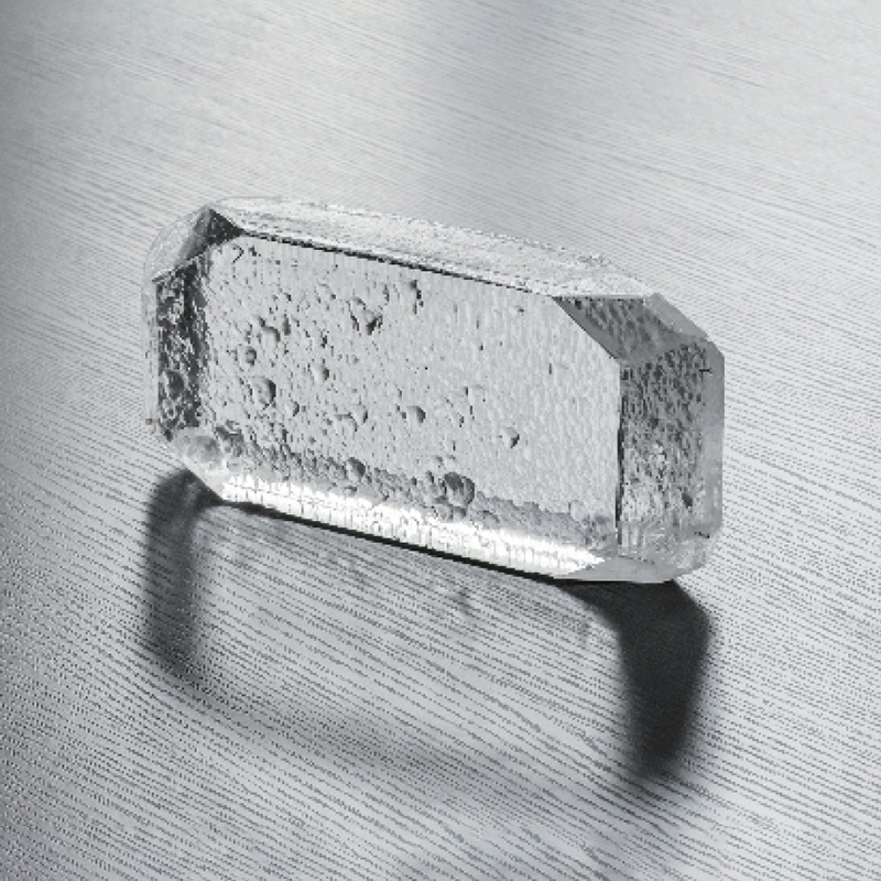

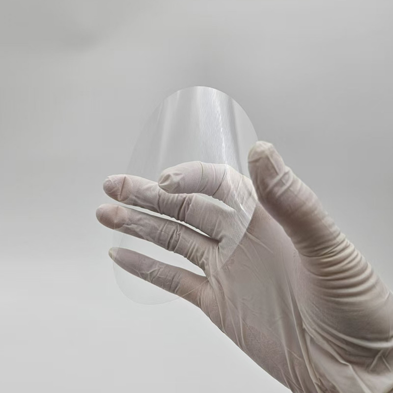

Corning Eagle XG Glass Wafer
Glass Wafer

-
+86-17701852595 WhatsApp
-
sales@plutosemitech.com Email
The Eagle XG Glass Wafer is a high-performance glass wafer manufactured by Corning. It is made from Corning's Eagle XG Glass, an alkali-free boroaluminosilicate glass widely used in advanced display, optics, and semiconductor applications. Eagle XG Glass is known for its exceptional surface flatness, high dimensional stability, a thermal expansion coefficient matched to silicon, excellent optical clarity, and an environmentally friendly composition free of heavy metals. These properties make it an ideal substrate material for thinner, more flexible, and lighter display panels, as well as for semiconductor processing and scientific applications.

Corning Eagle XG Glass Wafer Specifications
| Product Name | Eagle XG Glass Wafer |
| Size | 2/4/6/8/12inch or customized |
| Package | Hundred-class clean room |
| Customized Support | YES |
| RoHS | YES |
| Delivery Methods | Logistics Express |
| Marketable Area | oversea |
| Growth Method | Composite |
| Base | SiO2 |
| Dielectric Constant(k=EO/E) | 5-6 |
| Refractive(@589.3nm) | 1.50-1.52 |
| Mechanical property | |
| Item | Value |
| Density ρ (25 °C) | 2.3-2.5 g/cm3 |
| Poisson's ratio | 0.20-0.25 |
| Vickers hardness HK0.2/25 | 640 |
| Thermal property | |
| Item | Value |
| Thermal Expansion (0 to 300℃) | 3-3.5(ppm/C) |
| Strain Point (°C) | 650-700 |
| Anneal Point | 700-750 |
| Diameter | 2inch | 3inch | 4inch | 5inch | 6inch | 8inch | 12inch |
| Thickness (um) | Depends on Request | ||||||
| Material | Eagle XG | ||||||
| Grade/Brand | Corning | ||||||
| Surface Finished | DSP、SSP、DSL | ||||||
| TTV (um) | <5 | <5 | <5 | <5 | <5 | <10 | <15 |
| Bow/Warp (um) | <20 | <20 | <30 | <30 | <30 | <40 | <60 |
| Ra (nm) | <1 | ||||||
| S/D (um) | 40/20 | ||||||
| special indexes: Ultra-flat glass wafer: TTV<1um Ultra-thin glass wafer: Thickness:0.1-0.3um Ultra-smooth glass wafer: Ra≤0.2nm | |||||||
Corning Eagle XG Glass Wafer Features
1. Surface Flatness:
Eagle XG glass wafers boast exceptional surface flatness, with a total thickness variation (TTV) of less than 1 micron. This ultra-flat surface provides an ideal substrate for high-precision microelectronics manufacturing, ensuring exceptional accuracy and consistency during micro- and nanofabrication processes. Its surface roughness (Ra) of less than 1 nanometer is exceptional in the industry, meeting the most stringent process requirements.
2. Dimensional Stability:
Eagle XG glass wafers exhibit exceptional dimensional stability, with a coefficient of thermal expansion (CTE) of 3 to 3.5 ppm/°C from 0 to 300°C, closely matching that of silicon. This characteristic ensures Eagle XG glass wafers maintain their dimensions despite temperature fluctuations, reducing stress and deformation caused by thermal expansion mismatch, thereby improving product reliability and performance.
3. Optical Clarity:
Eagle XG glass wafers offer exceptional optical clarity, providing crystal-clear viewing. Its industry-leading optical performance makes it suitable for a variety of applications requiring high transparency, such as display panels and optical sensors. This high transparency makes Eagle XG glass wafers an ideal choice for manufacturing high-quality optical products.
4. Environmentally Friendly:
Eagle XG glass wafers utilize a heavy metal-free, environmentally friendly composition, meeting the stringent environmental protection requirements of modern manufacturing. This eco-friendly feature not only helps reduce environmental impact but also ensures product safety during use, complying with global environmental regulations and standards.
5. Mechanical Properties:
Eagle XG glass wafers exhibit excellent mechanical properties, with a Vickers hardness of 640 HK0.2/25, capable of withstanding high pressure and abrasion. This high strength enables Eagle XG glass wafers to maintain excellent performance in various complex manufacturing environments, reducing the risk of product failure due to mechanical damage.
6. Thermal Stability:
Eagle XG glass wafers offer excellent thermal stability, with a strain point between 650 and 700 degrees Celsius and an annealing point between 700 and 750 degrees Celsius. This high thermal stability enables Eagle XG glass wafers to maintain their structure and properties in high-temperature environments, making them suitable for manufacturing processes requiring high-temperature processing, such as semiconductor processing and microelectronics packaging.
7. Size Variety:
Eagle XG glass wafers are available in a variety of sizes, including 2-inch, 3-inch, 4-inch, 5-inch, 6-inch, 8-inch, and 12-inch, to meet diverse customer needs. Thickness can be customized to meet specific customer requirements, providing ultimate flexibility and adaptability for a variety of applications.
8. Surface Treatment:
Eagle XG glass wafers offer a variety of surface treatment options, including double-side polishing (DSP), single-side polishing (SSP), and double-side laser polishing (DSL). These surface treatments meet diverse process requirements and ensure optimal performance in a variety of applications.
Corning Eagle XG Glass Wafer Process Flow
1. Raw Material Selection:
The production of Eagle XG glass wafers begins with rigorous raw material selection. Corning uses high-quality boroaluminosilicate glass raw materials to ensure the product's essential properties. These raw materials are precisely formulated to meet Eagle XG glass wafers' requirements for heavy metal-free and high purity.
2. Melting and Forming:
During the melting process, the raw materials are melted at high temperatures to form a homogeneous glass melt. Corning employs advanced melting technology to ensure the purity and homogeneity of the molten glass. The melt is then formed into wafers of varying sizes through a precision forming process. This process requires precise control of temperature and pressure to ensure dimensional accuracy and surface quality.
3. Precision Machining:
Eagle XG glass wafers undergo a precision machining process, including dicing, grinding, and polishing. The dicing process ensures dimensional accuracy, while the grinding and polishing processes further enhance surface flatness and finish. Corning utilizes advanced processing equipment and technology to ensure that every Eagle XG glass wafer meets industry-leading surface quality standards.
4. Surface Treatment:
The surface treatment of Eagle XG glass wafers is a critical step in the production process. Depending on customer requirements, wafers can be treated with double-side polishing (DSP), single-side polishing (SSP), or double-side laser polishing (DSL). These surface treatments meet diverse process requirements and ensure optimal performance in a variety of applications.
5. Quality Inspection:
During the production process, Corning rigorously inspects Eagle XG glass wafers. Using advanced testing equipment and technology, wafers are thoroughly inspected for dimensions, flatness, optical properties, and mechanical properties. Only wafers that pass these rigorous inspections are packaged and delivered to customers, ensuring high product quality and reliability.
6. Packaging and Delivery: Eagle XG glass wafers are packaged using specialized anti-static and moisture-proof packaging materials to ensure safety and stability during transportation and storage. Corning provides global logistics services to ensure timely delivery of high-quality products.
Corning Eagle XG Glass Wafer Application
1. Microelectromechanical Systems (MEMS) and Electronics:
Eagle XG glass wafers play a vital role in the manufacture of microelectromechanical systems (MEMS) and electronic devices. They are used in wafer packaging and substrate carriers, and are favored for their excellent functionality and high reliability in harsh environments. In the medical device industry, Eagle XG glass wafers are used to create hermetic MEMS packages, ensuring long-term device stability and safety.
2. Semiconductor Manufacturing:
In semiconductor manufacturing, Eagle XG glass wafers serve as carrier substrates for the production of delicate and fragile semiconductor wafers. Their excellent chemical and thermal stability enables Eagle XG glass wafers to safely handle these thin and fragile semiconductor wafers while reducing costs and environmental impact.
3. Biotechnology:
Eagle XG glass wafers have a wide range of applications in the biotechnology field. Boroaluminosilicate glass is the preferred material for medical device glass due to its excellent resistance to high temperatures and radiation. Eagle XG glass wafers are also used in the manufacture of microfluidic chips. Through nanoimprint lithography, glass provides the required optical transparency as a substrate, making it a popular choice for cover layers in silicon-based devices.
4. Integrated Circuit Packaging:
Eagle XG glass wafers offer improved performance and cost-effectiveness in integrated circuit (IC) packaging. Through-glass vias (TGVS) and wafer-level cover glass (WLC) are improved packaging solutions that benefit from glass's specific properties, such as stiffness and a roughness below 0.5 nm RMS. Eagle XG glass wafers protect ICs from impact and corrosion while maintaining pins and leads that connect to external circuitry.
5. Display Technology:
Eagle XG glass wafers are used to manufacture thinner, more flexible, and lighter display panels, supporting advanced display technologies. Their high flatness and dimensional stability make Eagle XG glass wafers an ideal substrate material for high-quality display panels that meet the stringent performance and reliability requirements of modern display technology.
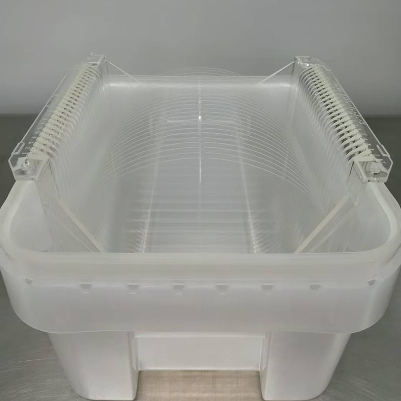
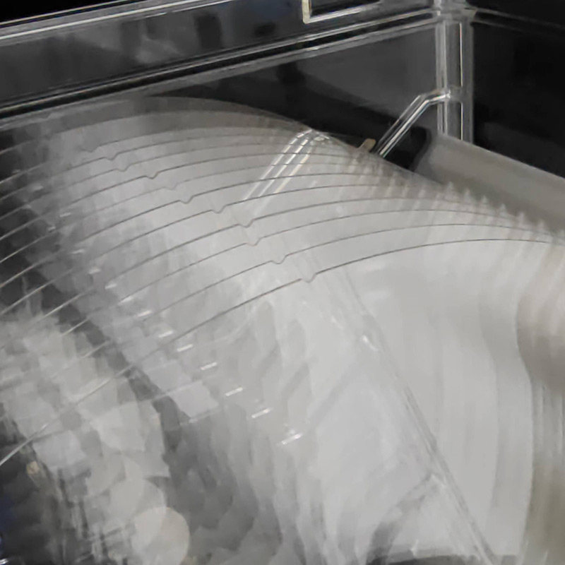
Packaging and Transportation
The packaging should be able to withstand the impact, vibration, stacking and extrusion that may be encountered during transportation, while also it has to easy to load, unload and handle.
We use professional wafer box packaging. The wafer box is protected by a double layer bag, the inside is a PE bag that can be dust-proof, and the outside is a aluminum foil bag that can be isolated from the air. The two-layer bags are vacuum-packed.
We will choose carton models according to different sizes of products. And between the product and the carton filled with shock-proof EPE foam, play a comprehensive protection.
Finally choose air transport to reach the customer's hands. This allows customers in any country and region to receive the product in the fastest time.
We comply with the Material Safety Data Sheet (MSDS) rules to ensure that the products transported are free of harmful substances and will not cause environmental pollution and explosion and other possible hazards.

Enterprise Strength
Factory Area: 3000 sq
Process:
1. Shaping→2. Edge Profile→3. Lapping→4. Polishing→5. Cleaning→6. Packing→7. Transportation
Capacity:
Glass Wafer --- 30K pcs
Silicon Wafer --- 20K pcs
(Equal to 6in)

Quality Assurance
Quality inspection method: Product inspection in accordance with SEMI standard or according to customer's requirements, together with product COA.
Warranty period: In accordance with the contract requirements.
Quality system management:
●Organize production according to ISO9001 and other quality system standards.
Quality management system and measures:
●Establish a strict quality assurance system, the heads of all departments and quality engineers to ensure the coordinated operation of the quality system.
●Strengthen the quality inspection system, strengthen the process quality control
●Strict material quality control, ensure that the input materials meet the design requirements and technical specifications.
●Implement a timely filing system for technical data to ensure that all processing technical data is complete/accurate.
Quality control in the production stage:
●Production preparation stage: carefully organize relevant personnel to learn product drawings and technical rules, and improve the technical level of employees.
●Quality control of the production process: the implementation of a strict handover system, the previous step of the process to the next step of the transfer, should be detailed processing. At the same time, strengthen the quality inspection system to ensure the quality of each step of the process.
●Quality acceptance: All processes must be quality acceptance before proceeding to the next process.

Pre-sales and After-sales
Pre-sales Service
Professional technical support and commercial team to help you determine product specifications according to product use, and issue specifications.
On-purchase Service
Produce products according to the confirmed specifications and our process.
After Sale Service
We will respond to any product problems encountered by customers or process problems encountered by customers within 24 hours. We can choose from various forms of service, such as email, video conference and so on.
Plutosemi Co., Ltd. was established in 2019, headquartered in Nanhai, Foshan, focusing on the research and development, production, and sales of high-performance semiconductor materials.
Advanced production capacity: We have three major production bases in China, with a monthly production capacity of 100000 equivalent 6-inch silicon wafers and 30000 equivalent 8-inch glass wafers, ensuring stable and efficient product supply for our customers.
High quality products: We provide efficient and stable product supply innovative solutions in the fields of glass wafers, silicon polishing wafers, epitaxial wafers (EPI), silicon on insulator wafers (SOI), and more. Our silicon wafers have the characteristics of ultra-thin, ultraflat, and high-precision, which can meet the needs of various high-end applications. Our glass and quartz substrates are also renowned for their high smoothness and precise aperture design.