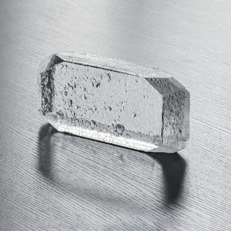

Quartz JGS2 Glass Wafer
Glass Wafer

-
+86-17701852595 WhatsApp
-
sales@plutosemitech.com Email
JGS2 Glass Wafer is an amorphous optical glass substrate made from high-purity silica as a base material. "JGS" is the classification mark for synthetic quartz glass in the Chinese national standard, and the number "2" represents a specific level of purity and optical performance. JGS2 glass wafers use a high-temperature melting process to convert high-purity quartz sand or vapor-deposited silica into a dense, transparent glass body, forming a disc-shaped substrate with an amorphous structure. This type of wafer does not introduce the directional arrangement required for single crystal growth during the manufacturing process, maintaining the isotropic properties of the glass material. As a basic substrate material, JGS2 glass wafers are widely used in process flows that require stable physical and chemical properties. They are not electrically conductive and are suitable for use as insulating layers or optical windows.

Product Name: Quartz JGS2 Glass Wafer
Size: 2/4/6/8/12inch or customized
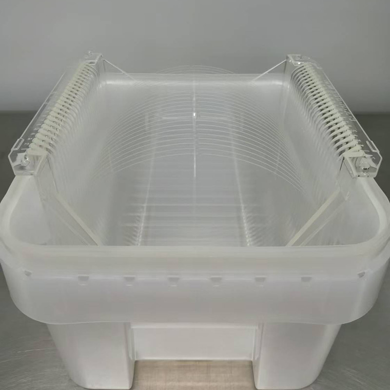
Package: Hundred-class clean room
Customized Support: YES
RoHS: YES
Delivery Methods: Logistics Express
Marketable Area: oversea
Growth Method: Electrofusion
Base: SiO2
Density: 2.2g/cm³
Melting Point: 1730℃
Moh's Hardness: 7
Maximum safe operating temperature (continuous): 1000-1100℃
Maximum safe operating temperature (short time): 1300-1400℃
Resistance to rapid change in temperature: 800-1100℃
Thermal Expansion Coefficient: 5.4×10⁻⁷
Dislectric Constant(0~106 Hz): 3.7(Normal Temperatures)
Conductivity(S/m): 10-17~10-16(20℃)
Color: Transparent
Quartz JGS2 Glass Wafer Specifications
| Grade | Product Name | Applied spectral band range(um) |
| JGS2 | Quartz Glass Wafer | 0.22-2.5 |
JGS2 Quartz Glass Wafer Transmittance
| Classification | Transmittance of 10mm thick blanks(%) | ||
| 0.220um | 0.240um | 0.300um | |
| 1 | >80 | >75 | >80 |
| 2 | >75 | >70 | >75 |
| 3 | >65 | >70 | |
| Technical Specifications | |||||||
| Diameter | 2inch | 3inch | 4inch | 5inch | 6inch | 8inch | 12inch |
| Thickness (um) | Depends on Request | ||||||
| Material | Quartz | ||||||
| Grade/Brand | JGS2 | ||||||
| Surface Finished | DSP、SSP、DSL | ||||||
| TTV (um) | <5 | <5 | <5 | <5 | <5 | <10 | <15 |
| Bow/Warp (um) | <20 | <20 | <30 | <30 | <30 | <40 | <60 |
| Ra (nm) | <1 | ||||||
| S/D (um) | 40/20 | ||||||
Special Indexes:
Ultra-flat glass wafer: TTV<1um
Ultra-thin glass wafer: Thickness: 0.1-0.3um
Ultra-smooth glass wafer: Ra≤0.2nm
Quartz JGS2 Glass Wafer Features
1. High-Purity Material:
JGS2 Glass Wafer utilizes high-purity SiO₂ raw materials synthesized by the electrofusion method, with a main component content exceeding 99.9%, ensuring controlled background impurities. Its total metal ion content is less than 50 ppm, meeting the technical requirements for JGS2 grade specified in GB/T 3284-2019. With a density of 2.2 g/cm³, it boasts a dense, bubble-free structure and near-zero porosity. This material remains chemically inert even at high temperatures, seldom releasing impurities that could contaminate the process environment. JGS2 Glass Wafer's low oxygen vacancy concentration reduces aging effects under UV radiation, making it suitable for long-term optical systems. The raw materials undergo multi-stage purification and vacuum melting to eliminate internal stress sources and enhance overall uniformity.
2. Strong Thermal Stability:
JGS2 Glass Wafer exhibits excellent thermal performance, with a continuous operating temperature range of 1000–1100°C and a short-term temperature tolerance of 1300–1400°C, meeting the requirements of high-temperature annealing and sintering processes. Its coefficient of thermal expansion is 0.55×10⁻⁶/°C (20–320°C), resulting in minimal dimensional change with temperature. Its thermal shock resistance reaches 800–1100°C, allowing it to withstand extreme temperature fluctuations without cracking. This characteristic makes it suitable for semiconductor process chambers subject to rapid heating and cooling cycles. JGS2 Glass Wafer exhibits no microcracks after repeated thermal cycling, ensuring safe operation and longevity of the equipment.
3. Excellent Optical Transmittance:
JGS2 Glass Wafer exhibits excellent transmittance from 220nm to 2500nm, with a transmittance of at least 80% at 250nm, making it suitable for optical systems from the ultraviolet to the near-infrared. Its refractive index is 1.458 at 589.3nm, its Abbe number is approximately 67, and its dispersion is low. The internal hydroxyl content is controlled to less than 10ppm, minimizing the impact of the water absorption peak on infrared transmission. The JGS2 Glass Wafer's double-sided parallelism error is less than 10 seconds, ensuring a stable optical path. This optical performance meets the ISO 10110-3 requirements for optical components and is suitable for precision imaging and sensing applications.
4. Ultra-Smooth Surface:
JGS2 Glass Wafer achieves an ultra-smooth surface with an Ra of ≤0.2nm and a TTV of<1μm, meeting="" the="" requirements="" of="" nanoscale="" thin="" film="" deposition.="" using="" a="" dsp="">
5. High Mechanical Strength:
JGS2 Glass Wafer has a Mohs hardness of 7, a compressive strength exceeding 1100 MPa, and a flexural strength of 60 MPa, offering excellent wear and scratch resistance. It is also less susceptible to edge and surface damage during handling and clamping. Its elastic modulus is approximately 72 GPa, and its fracture toughness is moderate, allowing it to withstand certain external impacts. JGS2 Glass Wafer maintains minimal deformation during vacuum clamping and mechanical positioning, ensuring process repeatability. These mechanical properties meet the stringent requirements of automated wafer handling systems.
6. Excellent Electrical Insulation:
JGS2 Glass Wafer has a dielectric constant of 3.7 (0-10⁶Hz) at room temperature and a dielectric loss tangent below 4×10⁻⁴, demonstrating excellent electrical insulation properties. Its volume resistivity exceeds 10¹⁶Ω·cm, and its surface resistivity exceeds 10¹⁴Ω/sq, effectively blocking leakage current. These properties make it suitable for high-voltage isolation structures and capacitive sensor substrates. JGS2 Glass Wafer exhibits no significant polarization response under high-frequency electric fields, demonstrating high stability. It complies with the IEC 60672 classification standard for ceramic and glass insulating materials.
7. Flexible Size Customization:
JGS2 Glass Wafers support a full range of custom diameters from 2 to 12 inches, with thicknesses ranging from 0.1mm to several millimeters. Standard tolerances are ±0.1mm, with tolerances up to ±0.01mm for special applications. Edge chamfers are precision-controlled within 0.2–0.5mm to avoid stress concentration. JGS2 Glass Wafers can undergo secondary processing such as slotting, drilling, and thinning according to customer drawings, making them compatible with a variety of equipment interfaces. This size flexibility serves a wide range of research and low-volume, high-end applications.
8. Clean Packaging Guarantee:
JGS2 Glass Wafers are cleaned, inspected, and packaged in a Class 100 cleanroom environment, meeting Class 100 particle control standards. They are sealed with anti-static material to prevent contamination during transportation. Each wafer is individually placed in a dedicated carrier to prevent friction damage. JGS2 Glass Wafers are rinsed with IPA and dried with nitrogen before shipment, achieving surface cleanliness levels that meet SEMI F21 requirements. This packaging process ensures pristine surface conditions upon arrival at the customer's location.
Quartz JGS2 Glass Wafer Process Flow
1. During the raw material preparation stage, high-purity quartz sand or fumed silica powder with a purity of at least 99.99% is used. The raw materials undergo magnetic separation, acid washing, and high-temperature calcination to remove metallic impurities and organic matter. After drying, they are loaded into graphite crucibles according to the appropriate proportions and prepared for entry into the electric arc melting furnace. All operations are performed in a closed environment to prevent external contamination. The raw material particle size is controlled between 50–200 μm to ensure uniform melting. This stage determines the initial purity and hydroxyl content of the JGS2 Glass Wafer, which directly impacts the final optical properties.
2. The electric melting process is performed in an electric arc furnace under an inert atmosphere. The temperature is raised to above 1730°C to completely melt the SiO₂. The current intensity is controlled between 10–15 kA, and the melting time is maintained for 2–4 hours to ensure sufficient air bubble expulsion. The melt is then formed into a cylindrical billet in a rotating mold. The rotation speed and cooling rate are precisely controlled to reduce internal stress. This process complies with the GB/T 3284 standard, producing an amorphous glass body free of crystalline phases. The electric fusion method eliminates impurities and ensures uniform structure on the JGS2 Glass Wafer.
3. Wafer dicing uses a multi-wire diamond saw blade to slice the quartz rod into thin slices. The cutting speed is controlled at 1.2 m/s and the feed rate is 0.5 mm/min to minimize edge chipping and microcracks. The slice thickness tolerance is controlled within ±0.05 mm. After dicing, rough grinding is performed to remove approximately 20–30 μm of surface damage. Each wafer is numbered and tracked to ensure batch traceability. This step determines the initial geometric accuracy and surface integrity of the JGS2 Glass Wafer.
4. Precision polishing is performed using two processes: double-side polishing (DSP) and single-side polishing (SSP). A colloidal silica polishing slurry is used, with a pH maintained at 9.5–10.5 and a removal rate of approximately 1–2 μm/h. The polishing pad flatness is better than 0.5 μm, ensuring a TTV of less than 1 μm. The Ra value is gradually reduced to ≤ 0.2 nm, achieving a mirror-like surface finish. After polishing, the wafer undergoes ultrasonic cleaning and deionized water rinsing to remove residual particles. This process directly impacts the surface quality and optical performance of the JGS2 glass wafer.
5. Final testing includes parameters such as thickness, TTV, Ra, transmittance, and impurity content. Quantitative analysis is performed using white light interferometry, spectrophotometry, and ICP-MS. Qualified products are cleaned with IPA in a Class 100 cleanroom, dried with nitrogen, and then vacuum-packaged. The packaging material is anti-static and moisture-proof, and a test report is included with each box. JGS2 glass wafers are marked with dimensions and grades according to customer specifications. The entire process complies with the ISO 9001 quality management system to ensure product consistency and reliability.
Quartz JGS2 Glass Wafer Application
1. Reticle Wafers:
JGS2 Glass Wafers are widely used as reticle substrates in semiconductor photolithography. Their high flatness and low thermal expansion ensure precise, offset-free pattern transfer during UV exposure. As the support material for photomasks, these wafers must withstand multiple cleaning and coating cycles. The chemical stability of JGS2 Glass Wafers ensures long-term reliability. Its surface roughness (Ra) of<0.2nm reduces="" light="" scattering="" and="" improves="" image="" contrast.="" it="" is="" suitable="" for="" i-line="">
2. Optical Instrument Manufacturing:
In optical instrument manufacturing, JGS2 Glass Wafers are often used as high-end replacements for microscope slides and cover glasses. Their high transmittance and low fluorescence background make them suitable for fluorescence microscopy and confocal imaging. JGS2 Glass Wafers maintain thickness uniformity within ±1μm, minimizing image distortion. The material is resistant to acid and alkali cleaning and is reusable, reducing laboratory costs. Its sodium- and calcium-free nature prevents ion precipitation from interfering with biological samples, making it widely used in life science research.
3. Infrared Detector Window Material:
JGS2 Glass Wafer is used as a high-temperature observation window and infrared detector window material. It can operate for extended periods in environments exceeding 1000°C, making it suitable for industrial furnaces, heat treatment equipment, and combustion chamber monitoring. JGS2 Glass Wafer maintains excellent transmission in the 2.5μm wavelength band, enabling real-time monitoring with infrared thermal imagers. Its strong thermal shock resistance prevents cracking even under sudden temperature fluctuations. This application ensures safe operation and accurate data acquisition in high-temperature processes.
4. MEMS Devices:
In MEMS device manufacturing, JGS2 Glass Wafer serves as a bonding substrate and package cover. Its thermal expansion coefficient is close to that of silicon, enabling low-temperature anodic bonding. JGS2 Glass Wafer's high insulation and airtightness ensure a stable internal environment within the device. Its surface can be metallized to form conductive pathways. This material supports wafer-level packaging (WLP), improving production efficiency and reliability, and is suitable for products such as pressure sensors and gyroscopes.
5. Solar Cell R&D:
JGS2 Glass Wafer is used as a test substrate for transparent conductive films in solar cell R&D. Its broad spectral transmittance is suitable for evaluating the optoelectronic properties of TCO thin films such as ITO and AZO. The JGS2 Glass Wafer's surface smoothness reduces interfacial reflection losses, improving test accuracy. Its high-temperature resistance supports subsequent annealing processes. This substrate can be used for simulated module aging experiments, assessing film adhesion and stability, and promoting technological advancements in photovoltaic materials.
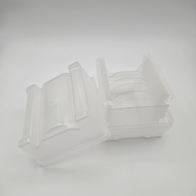
Packaging and Transportation
The packaging should be able to withstand the impact, vibration, stacking and extrusion that may be encountered during transportation, while also it has to easy to load, unload and handle.
We use professional wafer box packaging. The wafer box is protected by a double layer bag, the inside is a PE bag that can be dust-proof, and the outside is a aluminum foil bag that can be isolated from the air. The two-layer bags are vacuum-packed.
We will choose carton models according to different sizes of products. And between the product and the carton filled with shock-proof EPE foam, play a comprehensive protection.
Finally choose air transport to reach the customer's hands. This allows customers in any country and region to receive the product in the fastest time.
We comply with the Material Safety Data Sheet (MSDS) rules to ensure that the products transported are free of harmful substances and will not cause environmental pollution and explosion and other possible hazards.

Enterprise Strength
Factory Area: 3000 sq
Process:
1. Shaping→2. Edge Profile→3. Lapping→4. Polishing→5. Cleaning→6. Packing→7. Transportation
Capacity:
Glass Wafer --- 30K pcs
Silicon Wafer --- 20K pcs
(Equal to 6in)

Quality Assurance
Quality inspection method: Product inspection in accordance with SEMI standard or according to customer's requirements, together with product COA.
Warranty period: In accordance with the contract requirements.
Quality system management:
●Organize production according to ISO9001 and other quality system standards.
Quality management system and measures:
●Establish a strict quality assurance system, the heads of all departments and quality engineers to ensure the coordinated operation of the quality system.
●Strengthen the quality inspection system, strengthen the process quality control
●Strict material quality control, ensure that the input materials meet the design requirements and technical specifications.
●Implement a timely filing system for technical data to ensure that all processing technical data is complete/accurate.
Quality control in the production stage:
●Production preparation stage: carefully organize relevant personnel to learn product drawings and technical rules, and improve the technical level of employees.
●Quality control of the production process: the implementation of a strict handover system, the previous step of the process to the next step of the transfer, should be detailed processing. At the same time, strengthen the quality inspection system to ensure the quality of each step of the process.
●Quality acceptance: All processes must be quality acceptance before proceeding to the next process.

Pre-sales and After-sales
Pre-sales Service
Professional technical support and commercial team to help you determine product specifications according to product use, and issue specifications.
On-purchase Service
Produce products according to the confirmed specifications and our process.
After Sale Service
We will respond to any product problems encountered by customers or process problems encountered by customers within 24 hours. We can choose from various forms of service, such as email, video conference and so on.
Plutosemi Co., Ltd. was established in 2019, headquartered in Nanhai, Foshan, focusing on the research and development, production, and sales of high-performance semiconductor materials.
Advanced production capacity: We have three major production bases in China, with a monthly production capacity of 100000 equivalent 6-inch silicon wafers and 30000 equivalent 8-inch glass wafers, ensuring stable and efficient product supply for our customers.
High quality products: We provide efficient and stable product supply innovative solutions in the fields of glass wafers, silicon polishing wafers, epitaxial wafers (EPI), silicon on insulator wafers (SOI), and more. Our silicon wafers have the characteristics of ultra-thin, ultraflat, and high-precision, which can meet the needs of various high-end applications. Our glass and quartz substrates are also renowned for their high smoothness and precise aperture design.