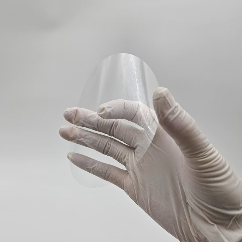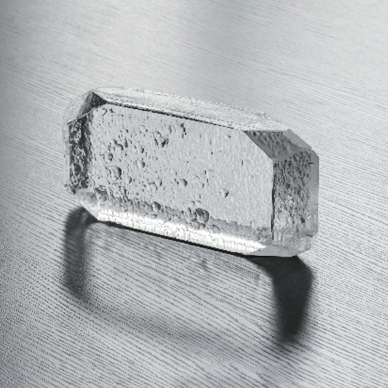
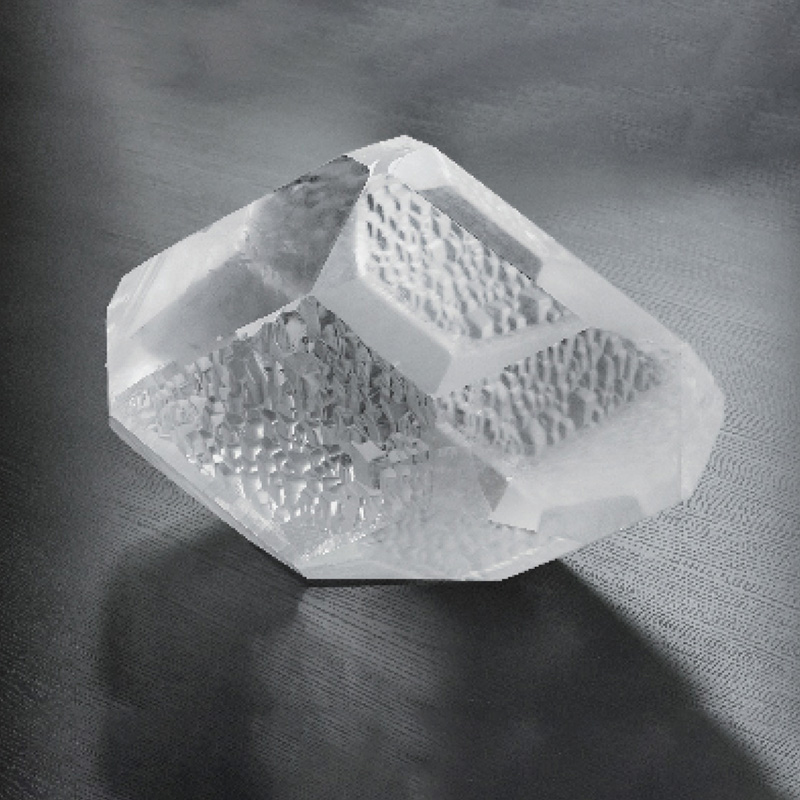
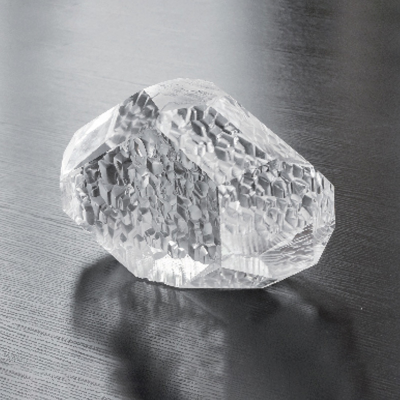
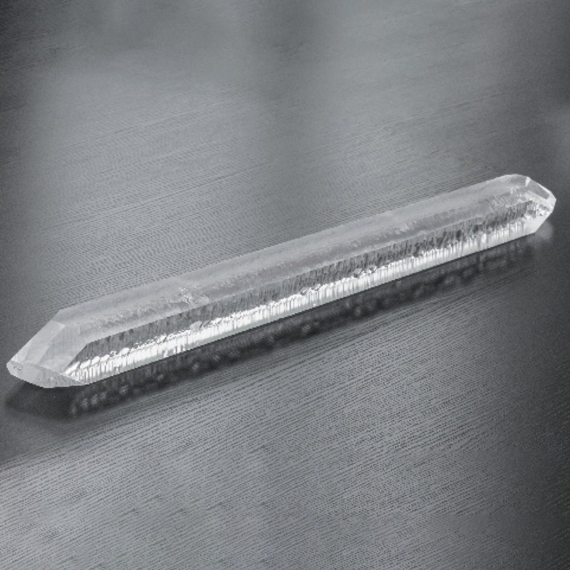
Single Crystal Glass Wafer
Glass Wafer

-
+86-17701852595 WhatsApp
-
sales@plutosemitech.com Email
Single crystal wafers are an essential building block in semiconductor manufacturing and the optical field. Produced through high-precision crystal growth techniques, they possess a high degree of crystal purity and a perfect crystal structure. The production process for single crystal silicon wafers requires strict temperature and pressure control to ensure uniform crystal growth and high quality. Due to their excellent physical and chemical properties, these materials are widely used in a variety of high-tech fields, including electronics, optics, and sensors. The production of single crystal silicon wafers requires highly sophisticated equipment and strict quality control to ensure that every wafer meets industry standards and customer requirements.
Single Crystal Glass Wafer Specifications
| Product Name | Single Crystal Wafer |
| Size2 | customized |
| PackageHundred | Hundred-class clean room |
| Customized Support | YES |
| RoHS | YES |
| Growth Method | Grown Crystal |
Physical properties of synthetic crystal quartz
| Density, g/cm³ | 2.65 |
| Melting point, °C | 1467 |
| Thermal conductivity, W/(m x K) (T = 25°C) | 10.7 (parallel to axis Z) 6.2 (perpendicular to axis Z) |
| Thermal coefficient of linear expansion at temperature range 0-25°, °C-1 | 7.1 10-6 (parallel to axis Z) |
| 13.2 10-6 (perpendicular to axis Z) | |
| Hardness (Mohs) | 7 |
| Specific heat capacity, J/(kg x K) (T = 25°C) | 710 |
| Dielectric constant at 30 MHz | 4.34 (parallel to axis Z) 4.27 (perpendicular to axis Z) |
| Young's modulus (E), GPa | 97.2 (parallel to axis Z) 76.5 (perpendicular to axis Z) |
| Shear modulus (G), GPa | 31.14 |
| Bulk modulus(K), GPa | 36.4 |
| Chemical stability | insoluble in water |
| Elastic coefficients | C11=87 C12=7 C44=58 C13=13 C14=18 C33=106 |
Synthetic crystal quartz refractive index vs wavelength
| l.mm | N0 | Ne | l.mm | N0 | Ne | l.mm | N0 | Ne |
| 0.185 | 1.676 | 1.69 | 0.243 | 1.605 | 1.617 | 0.589 | 1.544 | 1.553 |
| 0.194 | 1.66 | 1.673 | 0.263 | 1.593 | 1.604 | 1.083 | 1.534 | 1.543 |
| 0.204 | 1.643 | 1.656 | 0.291 | 1.581 | 1.591 | 1.8 | 1.524 | 1.532 |
| 0.219 | 1.625 | 1.637 | 0.34 | 1.567 | 1.577 | 2.5 | 1.512 | 1.52 |
| 0.231 | 1.614 | 1.626 | 0.405 | 1.557 | 1.567 | 3 | 1.5 | 1.507 |
Specification for lumbered quartz crystal
a) Angles:
i. Rotation angle of X-surface around Y-axis: 00°00’±15’
ii. Rotation angle of X-surface around Z-axis: 00°00’±15’
b) Dimensional tolerance:
i. Along X or Z axis:±0.1 mm
ii. Along Y axis:±10 mm
c) Surface roughness: as customized, lapped and polished are both available.
Single Crystal Glass Wafer Features
1. High-Purity Raw Materials:
This Single Crystal Glass Wafer uses quartz sand with a purity exceeding 99.999% as its starting material, ensuring extremely low impurity levels during the crystal growth process. This high purity directly determines the optical transmittance and electrical stability of the final Single Crystal Wafer. The raw materials undergo multiple acid washes and high-temperature calcination to remove metal ions and gaseous impurities. Before crystal growth, the raw materials are further dehydrated in a vacuum environment to prevent the introduction of hydroxyl groups (OH⁻) that could affect performance. This stringent control ensures that the Single Crystal Wafer exhibits excellent light transmittance from the UV to the IR, meeting the requirements of high-end optical and semiconductor applications. All batches are tested by ICP-MS to ensure compliance with RoHS environmental standards.
2. Precise Crystal Orientation:
The crystal orientation accuracy of the Single Crystal Wafer directly impacts its performance in optical and piezoelectric devices. The X-plane rotation angle around the Y and Z axes is controlled within 00°00'±15', complying with MIL-PRF-3083 standards. X-ray diffraction (XRD) monitors the cutting angle in real time to ensure consistent crystal orientation for each single crystal wafer. This precise orientation ensures predictable device frequency response and thermal expansion behavior. This tolerance range is suitable for high-stability oscillators and laser systems. All wafers undergo ingot orientation scanning before dicing to ensure repeatability and reliability in mass production, meeting the technical requirements of leading international equipment manufacturers.
3. Flexible Size Customization:
This single crystal wafer is available in standard 2-inch and 4-inch sizes, with custom sizes available upon request. Dimensional tolerances along the X and Z axes are controlled to ±0.1 mm, and along the Y axis up to ±10 mm, meeting diverse packaging and assembly requirements. Customization services include thickness, shape (round, square), and chamfer type. All customized solutions are process-verified based on customer drawings to ensure manufacturability.
4. Ultra-Low Surface Roughness:
Single crystal wafers achieve an ultra-smooth finish of Ra < 0.5 nm, supporting both lapping and polishing. The surface quality meets SEMI M1-0302 standards, making it suitable for high-reflectivity coatings and precision photolithography processes. Low roughness reduces light scattering losses, improving optical system efficiency. The polishing process utilizes wax-free mechanical chemical polishing technology to eliminate organic residues. Each wafer is inspected using a white-light interferometer to ensure full surface consistency.
5. Excellent Thermal Stability:
Single Crystal Wafer boasts a high melting point of 1467°C and a specific heat capacity of 710 J/(kg·K), maintaining structural stability over a wide temperature range. Its low coefficient of thermal expansion resists deformation at high temperatures, making it suitable for high-temperature process environments. It exhibited no cracking or warping during continuous 200°C thermal cycling testing. This thermal stability enables Single Crystal Wafer to be used in demanding applications such as high-temperature sensors and spacecraft optical windows. The material's uniform thermal conductivity avoids localized thermal stress concentrations. Its elastic moduli, such as C11=87 and C33=106, demonstrate its ability to maintain mechanical properties despite temperature fluctuations, ensuring long-term device reliability.
6. Excellent Chemical Inertness:
Single Crystal Wafer is composed of pure silicon dioxide, offering strong chemical stability, insolubility in water, and resistance to acid corrosion (except hydrofluoric acid). It withstands long-term immersion in a pH range of 1–12 without corrosion, making it suitable for wet etching and cleaning processes. This property ensures repeated use in semiconductor manufacturing without degradation. Certified according to ASTM C341 chemical resistance testing, it is suitable for use in strong acid and alkali processes. The surface of the Single Crystal Wafer resists contaminant absorption, simplifying cleaning.
7. High-Strength Structure:
Single Crystal Wafer boasts a Mohs hardness of 7 and a flexural strength exceeding 100 MPa, providing excellent mechanical durability. This high hardness reduces the risk of scratching and makes it suitable for automated handling and high-frequency vibration environments. A shear modulus of 58 GPa (C44) demonstrates strong resistance to shear deformation. In a drop test, a 4-inch wafer withstood a free fall from a height of 1.5 meters without breaking. This structural strength makes Single Crystal Wafer suitable for frequency components in mobile devices and automotive sensors. Finely chamfered edges prevent stress concentration and crack propagation, enhancing overall reliability.
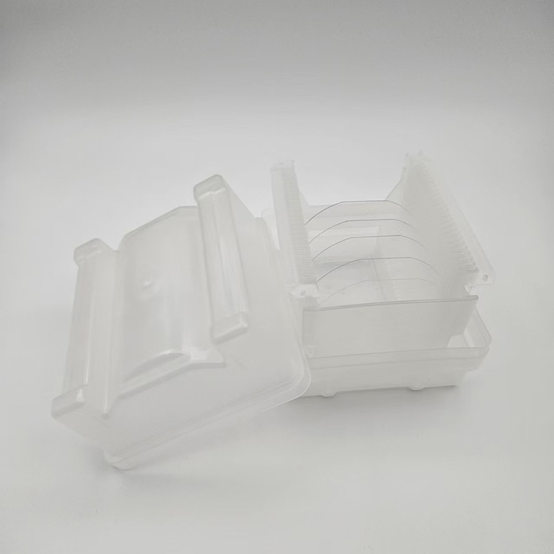
8. Clean Packaging Guarantee:
Each single crystal wafer is packaged in a Class 100 cleanroom and vacuum-sealed in anti-static, moisture-proof aluminum foil bags. The packaging environment is kept below ISO Class 4 to prevent particulate contamination. Shock-absorbing foam pallets are used during transportation to prevent damage from impact. The packaging label includes information such as batch number, dimensions, and crystal orientation, enabling full traceability. This packaging standard complies with JEDEC J-STD-033 requirements, ensuring that the single crystal wafer is ready for production line use upon delivery.
Single Crystal Glass Wafer Process Flow
1. Raw Material Purification:
Production begins with high-purity natural quartz sand, which undergoes multiple rounds of acid washing and high-temperature calcination to remove metal ions and organic impurities. A combined treatment with hydrochloric and hydrofluoric acids effectively dissolves harmful elements such as Al⁺ and Fe⁺. The resulting SiO₂ purity reaches over 99.999%, meeting the stringent raw material cleanliness requirements for single crystal growth. This process ensures the absence of heterogeneous nucleation during the melt, laying the foundation for subsequent crystal integrity and preventing internal defects that could impact the performance of the single crystal wafer.
2. Crystal Growth:
The raw material is heated to above 1467°C in a platinum crucible using the Czochralski method, resulting in a complete melt. A high-purity seed crystal is then slowly introduced into the melt, pulled and rotated at a constant rate of 0.5–2 mm/h to induce directional single crystal growth. The entire process is performed under an inert atmosphere to prevent oxidation and contamination. The growth process, which takes several days, results in a cylindrical ingot with a stable diameter, no grain boundaries, and a complete structure. This is the core guarantee of Single Crystal Wafer quality.
3. Ingot Orientation:
X-ray diffraction technology is used to scan the ingot surface for crystal orientation, precisely locating the X, Y, and Z axes. Cutting reference lines are marked on the ingot end face based on the customer's desired cutting angle (e.g., 00°00' ±15' around the Y axis on the X plane). Orientation accuracy is controlled within ±2', ensuring consistent crystal orientation for each Single Crystal Wafer and meeting the high-precision matching requirements of optical and piezoelectric applications.
4. Internal Slicing:
A diamond-coated internal circular saw blade is used to slice the ingot into thin slices, with slice thickness adjustable to within 0.2–1.0 mm. A constant feed rate and coolant circulation system are used during the slicing process to effectively reduce thermal stress and the risk of edge chipping. The equipment's highly rigid spindle ensures straight, uniform cuts, preserving the structural integrity and surface quality of the Single Crystal Wafer to the greatest extent possible.
5. Surface Lapping:
The cut wafers undergo double-sided lapping to remove surface damage and correct geometric deviations. Silicon carbide abrasives and metal lapping discs are used in multi-stage lapping under controlled pressure. Process parameters ensure thickness tolerances within ±0.01 mm and surface flatness reaching micrometer levels. This step provides a solid foundation for subsequent polishing, enhancing the overall dimensional accuracy and consistency of the single crystal wafer.
6. Chemical Mechanical Polishing:
Chemical mechanical polishing (CMP) technology is used to achieve atomically smooth surfaces. A colloidal silica polishing slurry and soft polyurethane pads are used to gradually eliminate micro-scratches and subsurface damage. The process consists of two stages: rough polishing and fine polishing, achieving a final surface roughness of Ra < 0.5 nm. The polished single crystal wafers exhibit high flatness, making them suitable for precision processes such as photolithography and coating.
7. Cleaning and Drying:
After polishing, the wafers undergo multiple steps, including ultrasonic cleaning, deionized water rinsing, IPA dehydration, and nitrogen drying. The cleaning process is performed in a Class 100 cleanroom to prevent particle contamination and water stains. Each single crystal wafer is handled individually to avoid cross-contamination. Cleanliness levels meet SEMI standards, ensuring that products are ready for use in high-end manufacturing lines upon delivery.
8. Inspection and Packaging:
Each single crystal wafer undergoes a comprehensive inspection, including key parameters such as thickness, warpage, surface roughness, and crystal orientation. Inspections are performed using white light interferometry, XRD, and microscopy. Qualified products are vacuum-sealed in anti-static aluminum foil bags and shock-proof packaging in a Class 100 cleanroom. Labels clearly indicate batch, specification, and technical parameters, ensuring full traceability and ensuring safe transportation and reliable operation of the single crystal wafers.
Single Crystal Glass Wafer Application
1. Heat Release Plate:
Single Crystal Wafer, with its high thermal conductivity and low coefficient of thermal expansion, is an ideal substrate for efficient heat dissipation. In high-power electronic devices, it rapidly conducts heat, preventing localized overheating and performance degradation. Its chemical stability ensures it will not oxidize or decompose even in high-temperature environments. It is suitable for devices with high thermal management requirements, such as laser diodes and power modules. The flat surface of the single crystal wafer facilitates close contact with the heat sink, improving heat transfer efficiency and extending device life.
2. Zero-Order Wave Plate:
Single Crystal Wafer can be used to fabricate zero-order wave plates due to its controllable and uniform birefringence. Precisely controlling thickness and crystal orientation enables precise phase retardation of polarized light. It is suitable for interferometers, laser systems, and optical sensing devices. Its high transmittance and low absorption loss ensure optical efficiency. The structural integrity of the single crystal wafer avoids the scattering issues common with polycrystalline materials, ensuring wavefront quality and improving system resolution and stability.
3. Trapezoidal Optical Sheet:
Trapezoidal optical sheets require materials with high geometric accuracy and optical uniformity. Single Crystal Wafers can be precisely cut and formed to meet complex design requirements. Their anisotropic optical properties enable directional control of the optical path, making them suitable for beam shaping and collimation systems. Polished surfaces achieve a mirror-like finish, reducing stray light. Single Crystal Wafers demonstrate excellent processing adaptability and performance consistency for this type of custom optical component and are widely used in laser projection and imaging equipment.
4. Shaped Optical Sheet:
Shaped optical sheets require materials with excellent processability and high optical quality. Single Crystal Wafers support a variety of custom shapes, such as hexagonal and elliptical. Their defect-free internal structure ensures distortion-free light transmission. They are suitable for high-end equipment such as aerospace optical systems and medical endoscopes. Through CNC precision cutting and edge polishing, Single Crystal Wafers can achieve high-precision molding of complex contours, meeting stringent assembly requirements and improving overall optical performance.
5. 49s Frequency Chip:
49s packaged frequency devices rely on the stability of the substrate material. Single crystal wafers, as resonator substrates, provide a stable dielectric environment and low loss. Their high Q factor supports high-precision frequency output. Frequency drift is less than ±3 ppm during aging testing. Single crystal wafers' low hygroscopicity prevents humidity from affecting performance, making them suitable for applications requiring high frequency stability, such as communication modules and clock sources, ensuring system synchronization accuracy.
6. SMD Frequency Chip:
SMD frequency chips require a miniaturized substrate and high reliability. Single crystal wafers can be processed into miniature substrates, making them suitable for surface mount packaging. Their high hardness and heat resistance support high-temperature reflow soldering processes. They maintain frequency stability within a temperature range of -40°C to +125°C. The dimensional accuracy of single crystal wafers ensures a good fit with solder pads, reducing soldering defects. They are widely used in real-time clocks and RF modules in consumer electronics and IoT devices.
7.3-Inch Wafer:
The 3-inch single crystal wafer size lies between 2-inch and 4-inch sizes, making it suitable for transitioning to medium-scale production lines. Its diameter is 76.2 mm, conforming to the SEMI standard wafer size range. Single Crystal Wafers can be used for R&D verification, small-batch production, or specific equipment adaptation. Even at this size, Single Crystal Wafers maintain excellent flatness and thickness consistency, supporting photolithography and coating processes, reducing R&D costs and improving trial production efficiency.
8. Square Piece:
Square wafers offer space-saving advantages in certain optical and sensor designs. Single Crystal Wafers can be customized in square or rectangular shapes with a side length tolerance of ±0.1 mm. Their right-angled edges facilitate alignment and packaging. They are suitable for applications such as array sensors and LED package substrates. The isotropic surface treatment of Single Crystal Wafers ensures consistent performance on all four sides, improving module integration and optical coupling efficiency.
9. Sensor Chip:
Single Crystal Wafers are widely used in pressure, temperature, and chemical sensors due to their high sensitivity and stability. Their piezoelectric effect and thermal conductivity properties enable precise response to environmental changes. The surface can be functionalized to enhance selectivity. Signal drift is minimal during long-term monitoring. Single Crystal Wafers are suitable for industrial automation, environmental monitoring, and other fields, providing a reliable data acquisition foundation and enhancing system intelligence.
10. LED Chip:
As a substrate material for LED epitaxial growth, Single Crystal Wafer provides an atomically flat growth interface. Its excellent lattice matching reduces dislocation density and improves luminous efficiency. Its high thermal conductivity helps dissipate heat from the chip, extending its lifespan. It is suitable for high-brightness LED and Mini/Micro LED manufacturing. The low defect density of Single Crystal Wafer ensures device yield and promotes the development of solid-state lighting technology.
11. Optical Sheet:
Optical sheets require materials with high transmittance and low birefringence. Single Crystal Wafer boasts a transmittance exceeding 90% from the UV to near-infrared range, making it suitable for components such as filters and windows. Its uniform structure minimizes image distortion and is suitable for AR and HR coatings. Single Crystal Wafer is widely used in precision instruments such as microscopes, telescopes, and spectrometers, improving the clarity and signal-to-noise ratio of optical systems.

Packaging and Transportation
The packaging should be able to withstand the impact, vibration, stacking and extrusion that may be encountered during transportation, while also it has to easy to load, unload and handle.
We use professional wafer box packaging. The wafer box is protected by a double layer bag, the inside is a PE bag that can be dust-proof, and the outside is a aluminum foil bag that can be isolated from the air. The two-layer bags are vacuum-packed.
We will choose carton models according to different sizes of products. And between the product and the carton filled with shock-proof EPE foam, play a comprehensive protection.
Finally choose air transport to reach the customer's hands. This allows customers in any country and region to receive the product in the fastest time.
We comply with the Material Safety Data Sheet (MSDS) rules to ensure that the products transported are free of harmful substances and will not cause environmental pollution and explosion and other possible hazards.

Enterprise Strength
Factory Area: 3000 sq
Process:
1. Shaping→2. Edge Profile→3. Lapping→4. Polishing→5. Cleaning→6. Packing→7. Transportation
Capacity:
Glass Wafer --- 30K pcs
Silicon Wafer --- 20K pcs
(Equal to 6in)

Quality Assurance
Quality inspection method: Product inspection in accordance with SEMI standard or according to customer's requirements, together with product COA.
Warranty period: In accordance with the contract requirements.
Quality system management:
●Organize production according to ISO9001 and other quality system standards.
Quality management system and measures:
●Establish a strict quality assurance system, the heads of all departments and quality engineers to ensure the coordinated operation of the quality system.
●Strengthen the quality inspection system, strengthen the process quality control
●Strict material quality control, ensure that the input materials meet the design requirements and technical specifications.
●Implement a timely filing system for technical data to ensure that all processing technical data is complete/accurate.
Quality control in the production stage:
●Production preparation stage: carefully organize relevant personnel to learn product drawings and technical rules, and improve the technical level of employees.
●Quality control of the production process: the implementation of a strict handover system, the previous step of the process to the next step of the transfer, should be detailed processing. At the same time, strengthen the quality inspection system to ensure the quality of each step of the process.
●Quality acceptance: All processes must be quality acceptance before proceeding to the next process.

Pre-sales and After-sales
Pre-sales Service
Professional technical support and commercial team to help you determine product specifications according to product use, and issue specifications.
On-purchase Service
Produce products according to the confirmed specifications and our process.
After Sale Service
We will respond to any product problems encountered by customers or process problems encountered by customers within 24 hours. We can choose from various forms of service, such as email, video conference and so on.
Plutosemi Co., Ltd. was established in 2019, headquartered in Nanhai, Foshan, focusing on the research and development, production, and sales of high-performance semiconductor materials.
Advanced production capacity: We have three major production bases in China, with a monthly production capacity of 100000 equivalent 6-inch silicon wafers and 30000 equivalent 8-inch glass wafers, ensuring stable and efficient product supply for our customers.
High quality products: We provide efficient and stable product supply innovative solutions in the fields of glass wafers, silicon polishing wafers, epitaxial wafers (EPI), silicon on insulator wafers (SOI), and more. Our silicon wafers have the characteristics of ultra-thin, ultraflat, and high-precision, which can meet the needs of various high-end applications. Our glass and quartz substrates are also renowned for their high smoothness and precise aperture design.