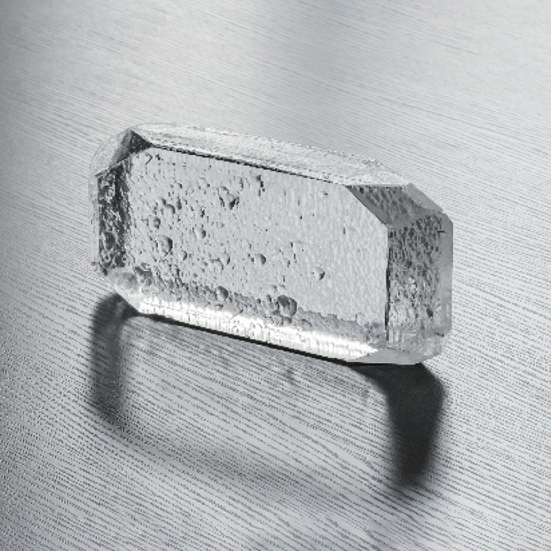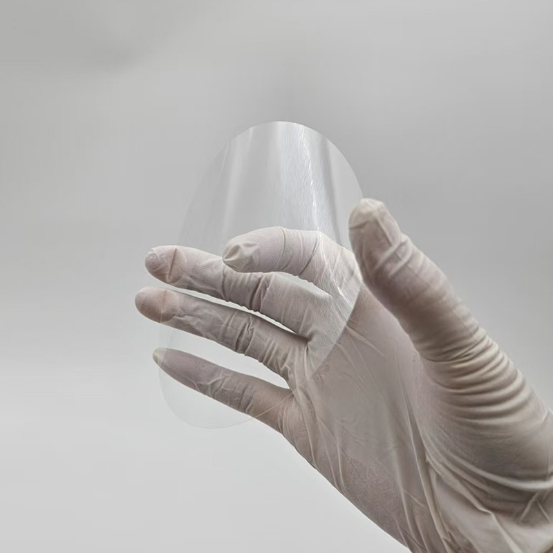

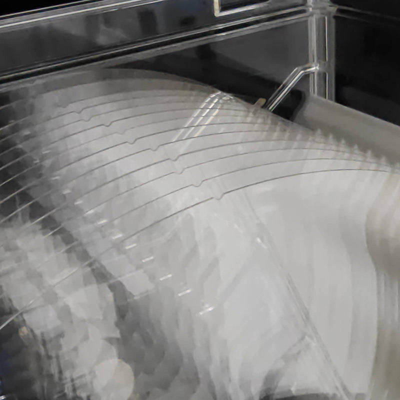
SK-1300 Glass Wafer
Glass Wafer

-
+86-17701852595 WhatsApp
-
sales@plutosemitech.com Email
SK-1300 Glass Wafer is a high-purity synthetic fused quartz wafer produced using advanced manufacturing processes. It is known for its extremely low hydroxyl content (<200ppm) and excellent optical and thermal properties. The product is based on a SiO₂ substrate, has no fluorescence (at 254nm wavelength), a density of 2.2g/cm³, a Poisson's ratio of 1.1, a Vickers hardness of 55, and a thermal expansion coefficient as low as 5.5×10⁻⁷. These characteristics make it have a wide range of application potential in semiconductor manufacturing, optical component production and other fields.

SK-1300 Glass Wafer Specifications
| Mechanical property | |
| Item | Value |
| Density ρ (25 °C) | 2.2g/cm³ |
| Poisson's ratio | 1.1 |
| Vickers hardness | 55 |
| Thermal property | |
| Item | Value |
| Thermal Expansion | 5.5*10⁻⁷ |
| Strain Point (°C) | 1700 |
| Anneal Point | 1060 |
| Diameter | 2inch | 3inch | 4inch | 5inch | 6inch | 8inch | 12inch |
| Thickness (um) | Depends on Request | ||||||
| Material | SK1300 | ||||||
| Grade/Brand | Ohara | ||||||
| Surface Finished | DSP、SSP、DSL | ||||||
| TTV (um) | <5 | <5 | <5 | <5 | <5 | <10 | <15 |
| Bow/Warp (um) | <20 | <20 | <30 | <30 | <30 | <40 | <60 |
| Ra (nm) | <1 | ||||||
| S/D (um) | 40/20 | ||||||
Special Indexes:
Ultra-flat glass wafer: TTV<1um
Ultra-thin glass wafer: Thickness:0.1-0.3um
Ultra-smooth glass wafer: Ra≤0.2nm
SK-1300 Glass Wafer Features
1. High purity:
SK-1300 Glass Wafer uses high-purity synthetic fused quartz material, which is much purer than materials produced by traditional direct methods. This high purity property enables it to effectively reduce impurity contamination during semiconductor manufacturing and improve chip yield and performance stability. For example, in the photolithography process, high-purity wafers can avoid photolithography defects caused by impurities and ensure accurate pattern transfer.
2. Low hydroxyl content:
The hydroxyl content of this wafer is extremely low, less than 200ppm. Low hydroxyl content helps improve the optical performance of the wafer, especially the transmittance in the ultraviolet region. This is critical for semiconductor manufacturing that requires high-precision optical measurement and photolithography processes, ensuring uniform exposure and precise patterning of photoresists.
3. Excellent thermal stability:
The thermal expansion coefficient of SK-1300 Glass Wafer is only 5.5×10⁻⁷, which is much lower than that of ordinary glass materials. This low thermal expansion coefficient enables it to maintain dimensional stability during high-temperature processing and reduce deformation and cracks caused by thermal stress. For example, during the high-temperature diffusion and annealing process of semiconductor chips, the wafer can remain flat, ensuring the smooth progress of subsequent processes.
4. High hardness:
The Vickers hardness of this wafer reaches 55, which has high wear resistance and scratch resistance. In the semiconductor manufacturing process, the wafer needs to be handled and processed many times. High hardness can effectively prevent scratches and damage on the surface of the wafer, extend the service life of the wafer, and reduce production costs.
5. High density:
The density of SK-1300 Glass Wafer is 2.2g/cm³. This high density property gives it good mechanical strength and stability. In semiconductor manufacturing, high-density wafers can better withstand mechanical stress during processing, reduce damage caused by vibration and impact, and ensure the smooth progress of the production process.
6. Low Poisson's ratio:
The Poisson's ratio of this wafer is 1.1, which means that the lateral deformation of the wafer is small when subjected to external force. This feature is very important in semiconductor manufacturing, especially in lithography and etching processes, which can ensure the precise alignment and transfer of patterns and improve the yield and performance consistency of chips.
7. High strain point and annealing point:
The strain point of SK-1300 Glass Wafer is 1700°C and the annealing point is 1060°C. These high-temperature characteristics enable it to maintain good mechanical and optical properties in high-temperature environments, and are suitable for semiconductor manufacturing processes that require high-temperature processing, such as high-temperature diffusion and annealing.
8. Customized service:
This product supports customization and can provide wafers of different sizes (2/3/4/5/6/8/12 inches or customized sizes) and different surface treatments (DSP, SSP, DSL) according to customer needs. This customized service can meet the specific needs of different customers and improve the market competitiveness of products.
SK-1300 Glass Wafer Process Flow
1. Synthetic Fused Silica Technology:
SK-1300 Glass Wafer is produced using synthetic fused quartz technology, which ensures high purity and low hydroxyl content of the wafer. Through an advanced melting process, high-purity quartz raw materials are melted and formed at high temperatures to form wafers with excellent optical and thermal properties.
2. VAD Manufacturing:
The wafer is manufactured using VAD (Vapor Axial Deposition), an advanced manufacturing process that produces high-purity, low-hydroxyl synthetic fused quartz. VAD gradually deposits quartz material in the axial direction through vapor deposition to form high-quality wafers.
3. High-Temperature Treatment:
During the production process, SK-1300 Glass Wafer is treated with high temperatures to ensure that it has high strain points and annealing points. This high-temperature treatment process improves the thermal stability and mechanical properties of the wafer, enabling it to maintain good performance in high-temperature environments.
4. Precision Machining:
The wafer is precision machined and can be provided in different sizes and surface treatments according to customer needs. Through high-precision cutting, grinding and polishing processes, the dimensional accuracy and surface quality of the wafer are ensured to meet the needs of different application fields.
5. Quality control system:
The quality control system is strictly followed in the production process of SK-1300 Glass Wafer to ensure that each wafer meets industry standards and customer requirements. Through strict quality testing and control, key parameters such as wafer purity, hydroxyl content, thermal expansion coefficient, etc. are ensured to be within the specified range.
6. Environmentally friendly production:
The production process of this wafer complies with the RoHS standard to ensure that the impact of the product on the environment during production and use is minimized. By adopting environmentally friendly materials and processes, SK-1300 Glass Wafer not only has excellent performance, but also meets environmental protection requirements.
SK-1300 Glass Wafer Application
1. Semiconductor manufacturing:
SK-1300 Glass Wafer is widely used in semiconductor chip manufacturing, especially in key processes such as lithography, etching and diffusion. Its high purity, low hydroxyl content and excellent thermal stability can ensure high precision and high yield in the chip manufacturing process.
2. Optical component production:
The wafer can be used to produce high-precision optical components such as lenses, prisms and reflectors. Its excellent optical properties and low thermal expansion coefficient can meet the application requirements of optical components in high-precision optical systems.
3. Optical communication field:
In the field of optical communication, SK-1300 Glass Wafer can be used to manufacture optical communication devices such as optical waveguides and optical fiber connectors. Its high purity and low hydroxyl content can improve the optical performance and reliability of optical communication devices.
4. Micro-electromechanical systems (MEMS):
SK-1300 Glass Wafer is suitable for the manufacture of micro-electromechanical systems (MEMS), such as sensors and actuators. Its high hardness and good mechanical properties can ensure the stable operation of MEMS devices in complex environments.
5. Display technology:
The wafer can be used to manufacture high-precision display panels, such as OLED and LCD displays. Its excellent optical properties and thermal stability can improve the display effect and service life of the display panel.
6. Scientific research:
SK-1300 Glass Wafer is also widely used in scientific research, such as physical experiments and material research. Its high purity and excellent physical properties can provide a reliable experimental platform for researchers.
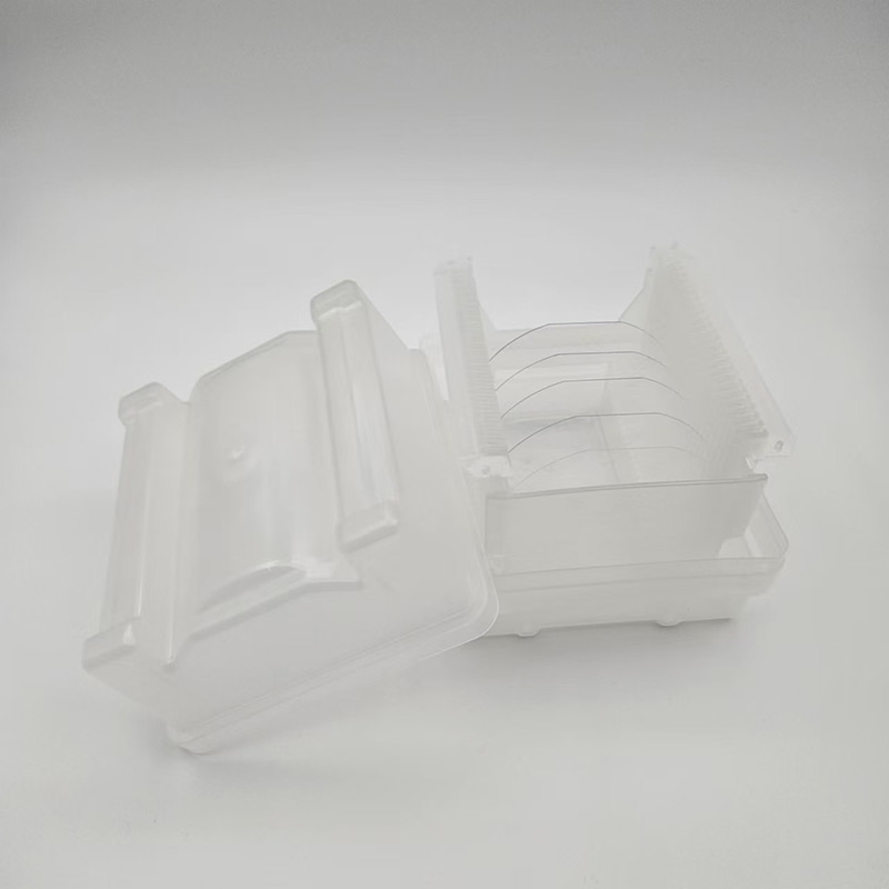
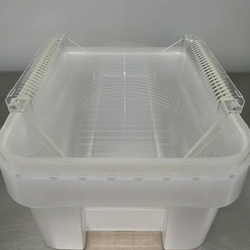
Packaging and Transportation
The packaging should be able to withstand the impact, vibration, stacking and extrusion that may be encountered during transportation, while also it has to easy to load, unload and handle.
We use professional wafer box packaging. The wafer box is protected by a double layer bag, the inside is a PE bag that can be dust-proof, and the outside is a aluminum foil bag that can be isolated from the air. The two-layer bags are vacuum-packed.
We will choose carton models according to different sizes of products. And between the product and the carton filled with shock-proof EPE foam, play a comprehensive protection.
Finally choose air transport to reach the customer's hands. This allows customers in any country and region to receive the product in the fastest time.
We comply with the Material Safety Data Sheet (MSDS) rules to ensure that the products transported are free of harmful substances and will not cause environmental pollution and explosion and other possible hazards.

Enterprise Strength
Factory Area: 3000 sq
Process:
1. Shaping→2. Edge Profile→3. Lapping→4. Polishing→5. Cleaning→6. Packing→7. Transportation
Capacity:
Glass Wafer --- 30K pcs
Silicon Wafer --- 20K pcs
(Equal to 6in)

Quality Assurance
Quality inspection method: Product inspection in accordance with SEMI standard or according to customer's requirements, together with product COA.
Warranty period: In accordance with the contract requirements.
Quality system management:
●Organize production according to ISO9001 and other quality system standards.
Quality management system and measures:
●Establish a strict quality assurance system, the heads of all departments and quality engineers to ensure the coordinated operation of the quality system.
●Strengthen the quality inspection system, strengthen the process quality control
●Strict material quality control, ensure that the input materials meet the design requirements and technical specifications.
●Implement a timely filing system for technical data to ensure that all processing technical data is complete/accurate.
Quality control in the production stage:
●Production preparation stage: carefully organize relevant personnel to learn product drawings and technical rules, and improve the technical level of employees.
●Quality control of the production process: the implementation of a strict handover system, the previous step of the process to the next step of the transfer, should be detailed processing. At the same time, strengthen the quality inspection system to ensure the quality of each step of the process.
●Quality acceptance: All processes must be quality acceptance before proceeding to the next process.

Pre-sales and After-sales
Pre-sales Service
Professional technical support and commercial team to help you determine product specifications according to product use, and issue specifications.
On-purchase Service
Produce products according to the confirmed specifications and our process.
After Sale Service
We will respond to any product problems encountered by customers or process problems encountered by customers within 24 hours. We can choose from various forms of service, such as email, video conference and so on.
Plutosemi Co., Ltd. was established in 2019, headquartered in Nanhai, Foshan, focusing on the research and development, production, and sales of high-performance semiconductor materials.
Advanced production capacity: We have three major production bases in China, with a monthly production capacity of 100000 equivalent 6-inch silicon wafers and 30000 equivalent 8-inch glass wafers, ensuring stable and efficient product supply for our customers.
High quality products: We provide efficient and stable product supply innovative solutions in the fields of glass wafers, silicon polishing wafers, epitaxial wafers (EPI), silicon on insulator wafers (SOI), and more. Our silicon wafers have the characteristics of ultra-thin, ultraflat, and high-precision, which can meet the needs of various high-end applications. Our glass and quartz substrates are also renowned for their high smoothness and precise aperture design.