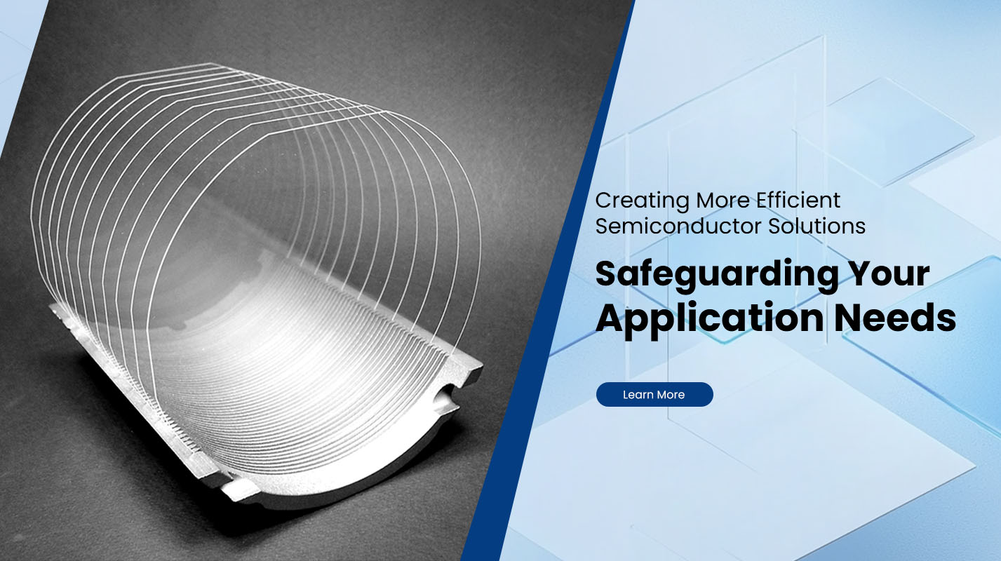
A silicon wafer is a thin, circular slice of single-crystal silicon used as the base material for building integrated circuits, sensors, power devices, MEMS structures, and many other semiconductor components. In practical production, it is the physical platform on which hundreds or thousands of chips can be created through repeated steps such as oxidation, deposition, lithography, etching, doping, and metallization.
-
2026-03-24
-
2026-03-23The core raw material for a solar wafer is high-purity silicon, and that silicon starts much earlier in the supply chain as quartz, which is silicon dioxide. In industrial production, quartz is reduced with carbon in an electric arc furnace to make metallurgical-grade silicon.
-
2026-03-19A solar wafer is the precision-cut silicon slice that becomes the foundation of a photovoltaic cell. Making it is not a simple cutting job. It is a tightly controlled material process that starts with purified polysilicon, continues through crystal growth and slicing, and ends with cleaning, sorting, and dimensional inspection.
-
2026-03-18Power conversion is under pressure to do more in less space. In modern chargers, inverters, industrial drives, renewable energy systems, and EV semiconductor platforms, engineers are expected to reduce switching loss, raise efficiency, handle higher voltage, and keep thermal behavior stable at the same time.
-
2026-03-17Choosing a reliable silicon wafer supplier is not only about unit price. In semiconductor manufacturing, wafer consistency affects device yield, downstream process stability, and delivery planning. Industry data from SEMI shows that worldwide silicon wafer shipments reached 12,973 million square inches in 2025, up 5.8 percent year over year, while revenue was about 11.4 billion US dollars.
-
2026-03-13Lithium niobate is an artificially synthesized crystal with the chemical formula LiNbO₃. It is not a naturally occurring mineral and must be produced in laboratories or industrial facilities through crystal growth techniques such as the Czochralski method.
-
2026-03-13Quartz (SiO₂) is resistant to acids, alkalis, and corrosion, making it suitable for use in harsh process environments. Quartz wafers feature an extremely low thermal expansion coefficient (approximately 0.55×10⁻⁶/℃), which is close to that of silicon (2.6×10⁻⁶/℃). This similarity significantly reduces thermal stress issues during semiconductor processes.
-
2026-02-11In the photovoltaic industry, the thickness of a solar wafer is not merely a dimensional specification—it represents a fundamental engineering compromise between material efficiency, mechanical stability, and electrical performance.
-
2026-02-10In semiconductor manufacturing, the physical flatness of silicon wafers is a fundamental determinant of yield and device performance. Two primary metrics—wafer bow and wafer warp—are used to quantify deviations from perfect flatness.
-
2026-02-09In the demanding world of semiconductor manufacturing, the purity of the silicon wafer substrate is non-negotiable. Even microscopic contaminants—be they particulate, organic, ionic, or metallic—can catastrophically disrupt the intricate patterning of integrated circuits...
-
2026-02-08Silicon wafers are the foundational substrate for virtually all semiconductor devices, from microprocessors to power electronics. Their cost is not a single figure but a complex variable determined by a multitude of factors.
-
2026-02-07In the semiconductor manufacturing ecosystem, epitaxial wafer services represent a fundamental and transformative technology that enables the creation of advanced electronic and photonic devices. Epitaxial processes involve the deposition of single-crystalline semiconductor layers onto wafer substrates...


