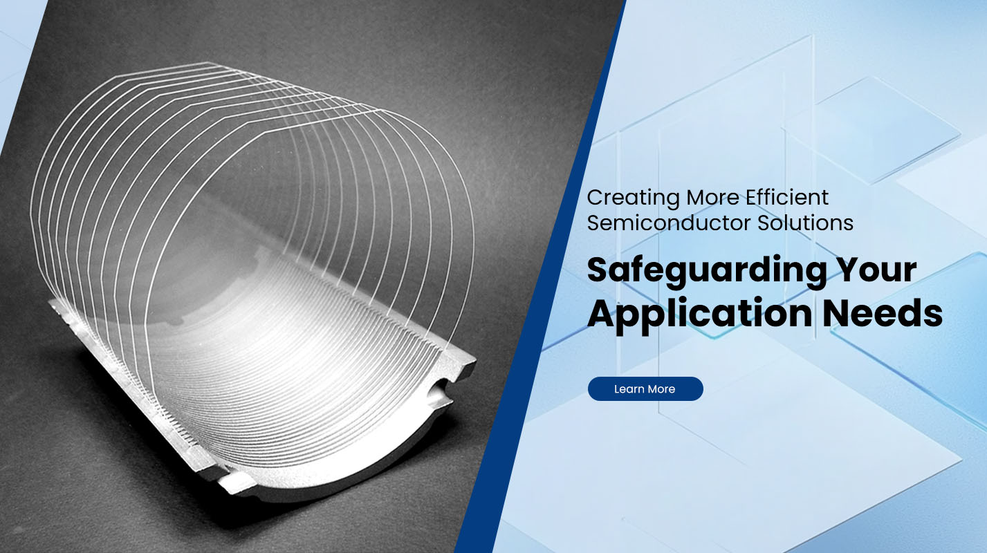
Wafer quality inspection is the cornerstone of semiconductor production, determining the yield, performance, and long-term reliability of every integrated circuit. For semiconductor manufacturers and suppliers, establishing a rigorous and multi-faceted inspection protocol is not just a quality control step...
-
2026-02-06
-
2026-02-05In the relentless pursuit of miniaturization and enhanced performance in electronics, Through-Glass Via (TGV) wafer technology has emerged as a foundational pillar for advanced packaging and integration. Moving beyond traditional silicon and organic substrates, TGV wafers utilize ultra-thin glass as a core material...
-
2026-02-04Silicon-on-Insulator (SOI) wafer technology represents a significant evolution in semiconductor manufacturing, offering distinct performance advantages over traditional bulk silicon substrates. At its core, an SOI wafer is a layered structure comprising a thin top layer of silicon, a buried silicon dioxide (SiO₂) insulating layer, and a silicon handle wafer substrate.
-
2026-02-03In the rapidly evolving world of renewable energy, solar wafers serve as the critical foundation of photovoltaic technology. These thin slices of semiconductor material, primarily silicon, are the essential component that converts sunlight directly into electricity.
-
2026-02-03In the world of advanced electronics and photonics, the substrate material is foundational. The choice between silicon and glass wafers is not merely a technical detail but a strategic decision that defines the performance, cost, and application scope of the final device.
-
2026-01-31Firstly, the smaller the values of these three parameters, the better. The larger the TTV, Bow, and Warp, the greater the negative impact on semiconductor manufacturing processes. Therefore, if the values of these three parameters exceed the standard, the silicon wafers will be scrapped.
-
2026-01-30Wafer foundry service is a specialized manufacturing service that turns a device concept into real silicon or other substrate-based wafers through controlled, repeatable semiconductor processes. Instead of building and operating a full fabrication line in-house.
-
2026-01-29Wafer flatness is not a single number. It is a set of geometry controls that protect your downstream process window, especially lithography focus margin, wafer bonding contact, and automated handling stability.
-
2026-01-28Compound semiconductor wafers are single-crystal substrates made from two or more elements rather than elemental silicon. They serve as the “starting platform” for building devices where silicon can struggle, such as high-power switching, high-frequency RF, optoelectronics, or advanced sensing.
-
2026-01-27Wafer thickness is not just a mechanical dimension. It directly influences handling yield, tool compatibility, lithography stability, grinding and polishing windows, and the risk of breakage during transport and processing.
-
2026-01-26Silicon carbide, commonly shortened to SiC, is not a metal. In materials science terms, SiC is best classified as a ceramic because it is a non-metallic, predominantly covalent-bonded compound made from silicon and carbon.
-
2026-01-24Silicon-on-Insulator, often shortened to SOI, is a wafer structure built from three functional layers: a top silicon device layer where circuits or microstructures are formed, an insulating buried oxide layer that electrically isolates the device layer, and a silicon handle wafer that provides mechanical strength during processing.


