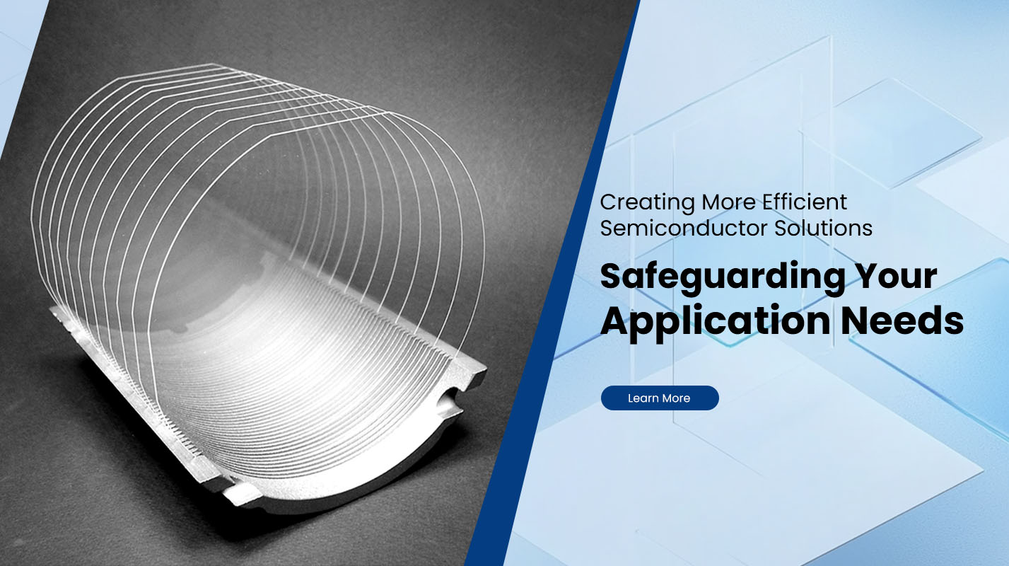
Silicon wafers look rigid, but they behave like precision optics in transit: any micro-scratch, edge chip, particle, moisture mark, or electrostatic event can turn a good wafer into a yield risk. Safe packing is not only about “getting it there.”
-
2026-01-23
-
2026-01-22Sapphire wafers are single-crystal aluminum oxide substrates that combine optical transparency, electrical insulation, chemical inertness, and high-temperature stability in one platform. That unique mix is why sapphire keeps showing up wherever devices must survive aggressive processes, tight lithography, or harsh operating environments.
-
2026-01-21When engineers ask “How much does a 300 mm silicon wafer weigh?”, they usually want a number that helps with tooling load limits, robot end-effector tuning, cassette logistics, and shipping design. The key point is that wafer weight is not a fixed constant—it depends primarily on thickness and (to a smaller extent) edge profile and special processing.
-
2026-01-20Silicon carbide, often shortened to SiC, is primarily used as the core material for high-efficiency power electronics. Its main role is to serve as a semiconductor wafer substrate that enables devices to switch and control electricity under higher voltage, higher temperature, and higher frequency conditions than conventional silicon can comfortably handle.
-
2026-01-16TSV stands for Through-Silicon Via, a semiconductor manufacturing process that creates vertical electrical connections straight through a silicon wafer or die. These tiny, conductive channels enable stacked chips to communicate directly and efficiently, which is a core enabler of advanced 3D and 2.5D integrated circuits.
-
2026-01-15In the semiconductor industry, standard wafer sizes refer to the diameter of the wafer, measured in millimeters (mm) or inches. This size defines fabrication tool compatibility, manufacturing throughput, and overall cost efficiency. Throughout industry evolution, wafer diameters have increased to support more device production per wafer and improve cost performance per chip.
-
2026-01-14Silicon wafers are standardized by diameter (inches or millimeters) and defined further by thickness and flatness to meet different device and packaging needs. In mainstream manufacturing today, wafers are typically 100 mm (4 in.), 150 mm (6 in.), 200 mm (8 in.), and 300 mm (12 in.) in diameter.
-
2026-01-13Silicon (Si) and silicon carbide (SiC) wafers are both foundational semiconductor substrates, but they serve very different engineering goals. In short, Si is the workhorse for mainstream logic, memory, sensors, and analog ICs due to its mature ecosystem and broad process compatibility, while SiC is a wide-bandgap material optimized for high-power, high-voltage, and high-temperature electronics where switching efficiency and thermal robustness are paramount.
-
2026-01-12Ceramic wafers are engineered, non-silicon substrates used in electronics, photonics, power modules, advanced packaging, and MEMS where electrical insulation, thermal stability, and mechanical strength are essential.
-
2026-01-08On December 31, 2025, PlutoSemi held a celebration to mark the recent completion of its manufacturing facility relocation and to welcome the upcoming New Year.
-
2026-01-07Lithium niobate, with the chemical formula LiNbO₃, is a versatile crystalline material that plays an essential role in modern photonics and electronics industries. As a wafer-form substrate, LiNbO₃ combines unique physical and optical characteristics with high stability to support a wide range of applications from telecommunications to sensing devices.
-
2026-01-06Silicon carbide wafers play a critical role in the evolution of modern power electronics. As industries demand higher efficiency, smaller system size, and greater reliability under extreme operating conditions, traditional silicon materials are increasingly limited.


