How to Avoid Damaging Silicon Wafers During Shipping?
Silicon Wafers are extremely sensitive components used across semiconductor manufacturing, MEMS fabrication, and advanced electronics. Even minor mechanical stress, particle contamination, or electrostatic discharge during transportation can result in micro-cracks, warpage, or surface defects that compromise yield. Proper shipping practices are therefore essential to protect wafer integrity from the fab to the end user.
Common Risks During Wafer Transportation
During shipping, silicon wafers face multiple risk factors that may not be visible immediately upon arrival. Mechanical shock from drops or vibration can cause edge chipping or internal stress fractures. Environmental exposure, including moisture and temperature fluctuation, may introduce oxidation or surface contamination. Electrostatic discharge can damage wafer structures at a microscopic level, especially for processed wafers with fine circuitry.
Understanding these risks is the first step toward building a reliable wafer shipping strategy.
Selecting Proper Wafer Carriers and Containers
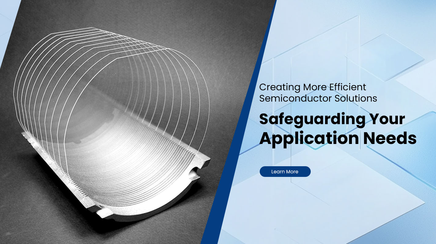
The choice of wafer carrier directly affects shipping safety. Rigid wafer cassettes designed for specific diameters help maintain precise spacing and prevent wafer-to-wafer contact. For higher-value or ultra-thin wafers, sealed single-wafer containers provide better isolation and mechanical stability.
Carriers should be manufactured from cleanroom-compatible materials with low particle generation and high dimensional stability. Poorly fitted or worn carriers can cause edge abrasion during transit, even under mild vibration.
Shock and Vibration Protection Strategies
External packaging plays a critical role in absorbing impact forces. Cushioning materials such as custom-cut foam inserts or suspension packaging help isolate wafer containers from external shocks. Double-boxing systems, with an inner protective case and an outer shock-absorbing carton, are commonly used for international shipping.
Packaging design should consider real transportation conditions, including truck vibration, air freight handling, and stacking pressure in logistics hubs.
Controlling Electrostatic Discharge and Contamination
Electrostatic discharge protection is essential, particularly for patterned or partially processed wafers. Antistatic bags, conductive containers, and grounding elements reduce charge buildup during handling and movement. Packaging materials should be selected to minimize static generation rather than relying solely on post-event discharge.
Cleanliness is equally important. Packaging environments should limit exposure to dust, fibers, and chemical residues. Sealed containers with controlled internal atmospheres help preserve wafer surface quality during long transit times.
Environmental Control During Shipping
Temperature and humidity variations can induce thermal stress or promote moisture-related defects. For long-distance or cross-climate shipments, insulated packaging combined with desiccants or humidity control packs helps maintain stable internal conditions.
Monitoring devices, such as shock or temperature indicators, provide valuable feedback on shipping performance and help identify potential weak points in the logistics process.
Best Practices for Handling and Logistics Coordination
Proper handling procedures reduce risk before wafers even enter the shipping box. Trained personnel should use gloves and vacuum tools designed for wafer handling to prevent edge damage and contamination. Clear labeling, orientation indicators, and handling instructions guide logistics providers in maintaining correct positioning throughout transit.
Coordination with experienced semiconductor logistics partners further reduces risk, as they understand the specific requirements of wafer transport and storage.
Working With Reliable Wafer Supply Partners
Shipping safety begins with suppliers who understand wafer sensitivity and packaging standards. Companies such as Plutosemi integrate wafer protection considerations into both manufacturing and delivery processes, offering properly packaged silicon wafers suitable for research, pilot production, and volume applications.
A supplier with strong process control and shipping expertise helps reduce downstream risk and supports consistent product quality.
Conclusion
Avoiding damage to silicon wafers during shipping requires a combination of proper carriers, protective packaging, environmental control, and disciplined handling practices. By addressing mechanical, electrostatic, and environmental risks at every stage of transportation, manufacturers and buyers can significantly reduce wafer loss and quality issues. Thoughtful logistics planning and cooperation with experienced wafer suppliers ensure that wafers arrive ready for immediate use, maintaining both performance and yield.
Previous: What are TTV, Bow, and Warp?


