


What are TTV, Bow, and Warp?
Bow, Warp, and TTV—three critical surface profile parameters of Silicon Wafers—are indispensable considerations in chip manufacturing. Collectively, these parameters characterize the flatness and thickness uniformity of silicon wafers, exerting a direct impact on numerous key processes in semiconductor fabrication.
What are TTV, Bow, and Warp?
TTV (Total Thickness Variation)
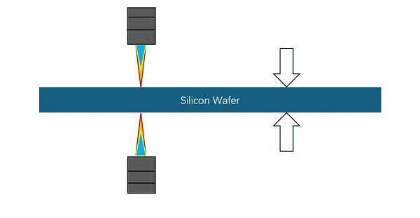
refers to the difference between the maximum thickness and minimum thickness of a silicon wafer. It serves as a core metric for evaluating the thickness uniformity of the wafer. In semiconductor manufacturing processes, the thickness of a silicon wafer must be highly consistent across its entire surface. TTV is typically calculated by measuring thickness at five distinct locations on the wafer, with the resulting value serving as a key criterion for assessing wafer quality.
Bow
In semiconductor fabrication, Bow denotes the curvature of a silicon wafer. The term likely derives from the curved shape of a bow. Bow value is defined as the maximum deviation between the center and the edge of the wafer, usually expressed in micrometers (µm). Per SEMI standards for 4-inch silicon wafers, the Bow value must be less than 30 µm.
Warp
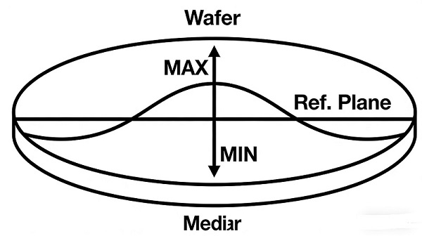
Warp is a global characteristic of a silicon wafer, representing the maximum distance that any point on the wafer surface deviates from a reference plane. It measures the vertical distance between the highest point and the lowest point across the entire wafer. SEMI standards specify that the Warp value for 4-inch silicon wafers should be less than 30 µm.
What are the differences between TTV, Bow, and Warp?
TTV focuses exclusively on thickness variation and is irrelevant to wafer bending or distortion. Bow characterizes overall curvature, primarily reflecting the height deviation between the wafer center and its edge. Warp provides a more comprehensive assessment, encompassing both the curvature and distortion of the entire wafer surface.