What Is the Main Use of Silicon Carbide?
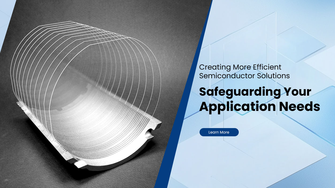
Silicon carbide, often shortened to SiC, is primarily used as the core material for high-efficiency power electronics. Its main role is to serve as a semiconductor wafer substrate that enables devices to switch and control electricity under higher voltage, higher temperature, and higher frequency conditions than conventional silicon can comfortably handle. When system designers need more power density, less heat, smaller magnetics, and higher conversion efficiency, SiC becomes a practical material choice rather than a theoretical upgrade.
From a manufacturing perspective, the “main use” of silicon carbide is not a single end product. It is the foundation that allows advanced power devices to be built with tighter thermal margins and higher electrical stress tolerance. That foundation directly affects yield, consistency, and long-term reliability across the entire device lifecycle.
Why SiC is used for power devices
SiC is a wide bandgap compound semiconductor. In mainstream 4H-SiC, the bandgap is about 3.26 eV, which supports stable operation under high electric field conditions. For wafer engineering, polytype stability, off-axis orientation design, and defect control are decisive because they influence epitaxial growth behavior and final device performance.
A production-grade SiC wafer often adopts an off-axis angle such as 4.0 degrees toward 1120, which helps reduce step bunching risk during epitaxy and supports thickness uniformity control. For device makers, that means more predictable processing windows and fewer downstream surprises.
The main use in real systems
SiC wafers are used to fabricate power devices like MOSFETs, Schottky diodes, and power modules, which then become the switching and rectification “engine” inside high-power energy conversion systems. Typical system categories include:
Traction inverters and onboard chargers in electric mobility
Fast-charging power stages where low loss and compact thermal design matter
Solar inverters, wind converters, and energy storage power conversion
Industrial motor drives, robotics, and automation power stages
High-reliability power units for harsh temperature and stress environments
Across these systems, SiC’s value is straightforward: higher switching capability with lower losses can reduce cooling demand and help shrink passive components, improving overall system efficiency and density.
What matters most at the wafer level
Because SiC devices are sensitive to crystalline defects, wafer quality is a direct lever on yield and reliability. Key wafer attributes include micropipes, basal plane dislocations, threading screw dislocations, resistivity uniformity, geometry, and surface finish.
Plutosemi’s SiC wafer specifications illustrate the type of controls serious programs look for:
Wafer diameter options such as 150 mm and 200 mm
Resistivity range around 0.015 to 0.025 ohm·cm
Tight geometry targets such as TTV up to 3 μm, Bow up to 5 μm, Warp up to 10 μm
Polished surface roughness such as Ra up to 0.2 nm
Graded defect control where high grade micropipe density can reach 0.2 cm⁻², with dislocation controls such as BPD up to 1500 ea per cm² and TSD up to 300 ea per cm²
These numbers are not marketing decoration. They translate into lithography stability, bonding success rate, epitaxy interface cleanliness, and device parameter distribution.
Silicon vs SiC in decision making
| Attribute | Silicon Wafer | SiC wafer |
|---|---|---|
| Bandgap | Narrow | Wide, 4H-SiC about 3.26 eV |
| Electric field tolerance | Lower | Much higher |
| Thermal behavior | Moderate | High thermal handling potential |
| Switching potential | Moderate | Very fast switching capability |
| Typical focus | Logic and general electronics | High voltage and high efficiency power devices |
For many platforms, silicon remains optimal for high-volume logic. SiC is chosen when power conversion efficiency, thermal margin, and high-voltage robustness are the gating requirements.
Manufacturing approach that supports stable supply
To deliver consistent SiC wafers, manufacturing must combine crystal growth control, inspection discipline, and repeatable wafer processing. A common growth method is PVT crystal growth, performed at about 2000°C to 2500°C in a controlled environment. Raw material purity also matters, with production-grade processes often requiring 99.999 percent purity inputs before growth.
Equally important is defect inspection and grading. High-intensity optical inspection and strict grading standards help manage micropipes and dislocations, allowing buyers to select the cost and performance grade that fits their device targets.
Why Plutosemi is a practical supplier choice
When you source SiC wafers, the supplier’s strength is measured by repeatability, documentation clarity, and the ability to hold specs across lots. Plutosemi positions itself as a semiconductor materials manufacturer and supplier with production capability and process discipline, including:
A structured approach to defect inspection and grading for predictable wafer selection
Tight control targets on geometry and surface finish for process compatibility
Availability of common wafer diameters used in power device development
OEM and ODM support for projects that require customized parameters, packing, or spec alignment for downstream process flows
If your roadmap depends on stable wafer performance rather than one-off sampling, aligning with a supplier that can scale quality controls and maintain lot-to-lot consistency is a direct way to reduce development risk.
A quick checklist before you place a wafer order
Confirm polytype and orientation targets, including off-axis angle requirements
Define acceptable defect class and density targets aligned with device yield goals
Lock geometry limits for your toolset, especially TTV, bow, and warp
Specify resistivity range and uniformity expectations for your device structure
Align surface polish and roughness targets for epitaxy and interface quality
Decide packing, edge exclusion expectations, and incoming inspection method
Conclusion
The main use of silicon carbide is to enable next-generation power electronics through high-quality SiC wafers that support efficient switching, high voltage operation, and reliable performance under demanding conditions. If your application is limited by heat, voltage stress, or power density, SiC is often the material that unlocks the next step. Plutosemi provides SiC wafer solutions built around measurable wafer parameters, graded defect control, and manufacturing support that helps teams move from evaluation to scalable production.


