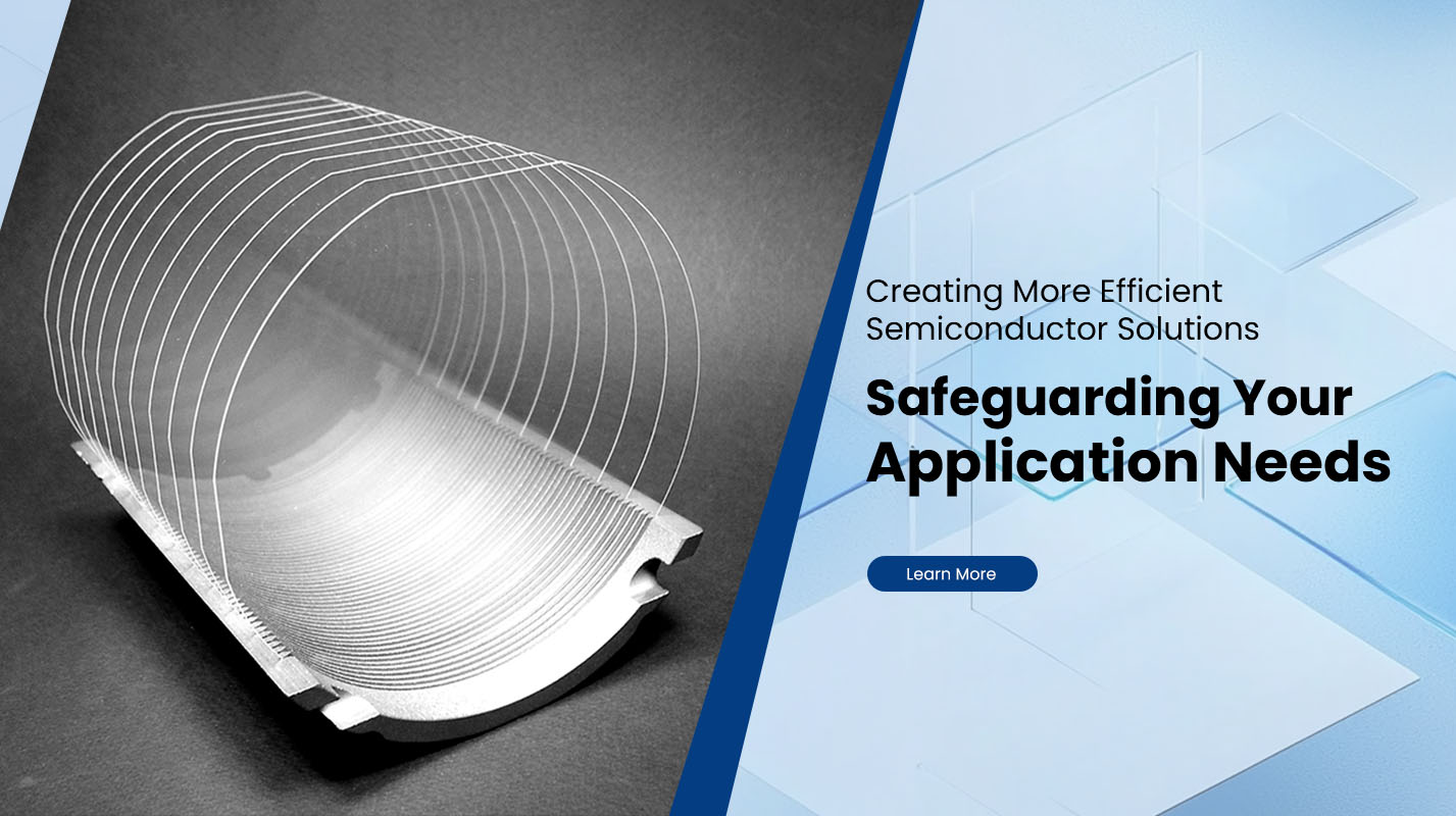
What Industries Use Sapphire Wafers?
Sapphire Wafers are single-crystal aluminum oxide substrates that combine optical transparency, electrical insulation, chemical inertness, and high-temperature stability in one platform. That unique mix is why sapphire keeps showing up wherever devices must survive aggressive processes, tight lithography, or harsh operating environments. For product teams and engineers, the real question is not whether sapphire works, but which industry requirements it matches best and how to specify orientation, thickness, and surface finish so downstream yield stays predictable.
LED and solid-state lighting
The most established volume use is as a substrate for nitride epitaxy in LED manufacturing. Sapphire’s thermal stability and proven compatibility with epitaxial growth make it a dependable base for GaN and related layers, including options like patterned sapphire when the process flow calls for light extraction improvements. When your priority is stable, repeatable epi behavior across lots, sapphire is often selected because its crystal consistency supports tight process windows and uniform deposition behavior.
Laser diodes and photonics components
Photonics applications value sapphire for two reasons that usually compete in other materials: broad optical transmission and mechanical durability. This makes sapphire suitable for optical windows, sensor covers, and wear-resistant transparent parts where surface damage and haze would quickly degrade performance. In UV and deep-UV optical paths, sapphire’s transparency and stability help maintain consistent optical throughput while surviving cleaning, temperature cycling, and long service life demands.
RF and microwave electronics
In high-frequency electronics, sapphire is used when isolation and low parasitic behavior matter. Its electrical insulating nature helps reduce unwanted coupling, while its stability supports fabrication steps that push temperature and chemical limits. Sapphire also appears in specialized substrates such as silicon-on-sapphire structures, where insulating behavior is used to suppress leakage and reduce parasitic capacitance in certain device approaches.
Sensors, MEMS, and harsh-environment instrumentation
Sapphire is widely chosen for sensing platforms and micro-structures that must operate under abrasion, pressure, corrosive media, or thermal shock. In these scenarios, hardness and chemical resistance matter as much as surface quality. A key practical advantage is that sapphire can be supplied in multiple orientations and polishing grades to align with your deposition and etch behaviors, then held to stable thickness for repeatable bonding, dicing, and packaging steps.
Consumer optics and protective covers
Wear resistance and optical clarity drive sapphire adoption in protective optical elements. Camera windows, protective sensor covers, and other transparent shields benefit from sapphire’s scratch resistance and long-term stability under daily contact and cleaning. This category is less about exotic epitaxy and more about consistent surface quality and low defect appearance, so flatness, haze control, and polishing selection become the purchasing focus.
Defense and aerospace optics
Defense-related systems use sapphire when both transparency and survivability are required, such as ruggedized windows and IR or UV optical elements exposed to mechanical wear and temperature extremes. In these builds, material traceability, repeatable inspection, and packaging cleanliness are often as important as the wafer itself, because field performance is sensitive to micro-scratches, particles, and edge chipping.
Research, quantum, and advanced electronics
Sapphire remains a staple in advanced R&D because it enables stable dielectric environments and repeatable thin-film processes. It is used in superconducting and quantum-adjacent device work where substrate loss, surface quality, and cleaning compatibility can be decisive. For research programs, flexibility matters: small squares for prototyping, nonstandard off-angles, and fast iteration on thickness and polish.
Matching industries to wafer specifications
Below is a practical mapping between common industry needs and the sapphire wafer specifications that typically matter most.
| Industry need | What to prioritize in the wafer spec | Typical outcome |
|---|---|---|
| Epitaxy for LEDs and nitride devices | Orientation control, epi-ready polishing, flatness consistency | More stable growth behavior and tighter yield distribution |
| Precision optics and windows | Optical-grade surface quality, low roughness, low defect appearance | Lower scatter and better long-term clarity |
| RF and microwave substrates | Electrical insulation stability, surface quality, thickness control | Reduced parasitics and more predictable high-frequency behavior |
| MEMS and sensors in harsh settings | Mechanical strength, chemical inertness, edge and thickness stability | Better survivability through fabrication and service life |
Why Plutosemi is a practical choice for sapphire wafer supply
From a manufacturing and supply standpoint, sapphire wafers succeed when the supplier can hold orientation, size, thickness, and polishing consistency across repeat purchases. Plutosemi’s sapphire wafer offering covers common planes such as C-plane, A-plane, M-plane, and R-plane, supports a wide range of standard sizes from small coupons to larger diameters, and provides polishing options including single-side polished, double-side polished, and epi-ready roughness control. Packaging is handled with cleanroom-oriented methods and clean bag practices to reduce particle risk in downstream processes. For projects that require customization, Plutosemi also supports OEM/ODM requirements and can align specifications to your drawing and process flow, including bulk order planning for ongoing programs.
Closing perspective
Sapphire wafers are not a niche material anymore. They are a cross-industry foundation where optical performance, insulation, durability, and high-temperature stability must coexist. The best results come from specifying the wafer as part of the process, not as a commodity line item: define the orientation, surface finish, thickness, and cleanliness level that your manufacturing steps demand, then lock those parameters with a supplier that can repeat them reliably at scale.


