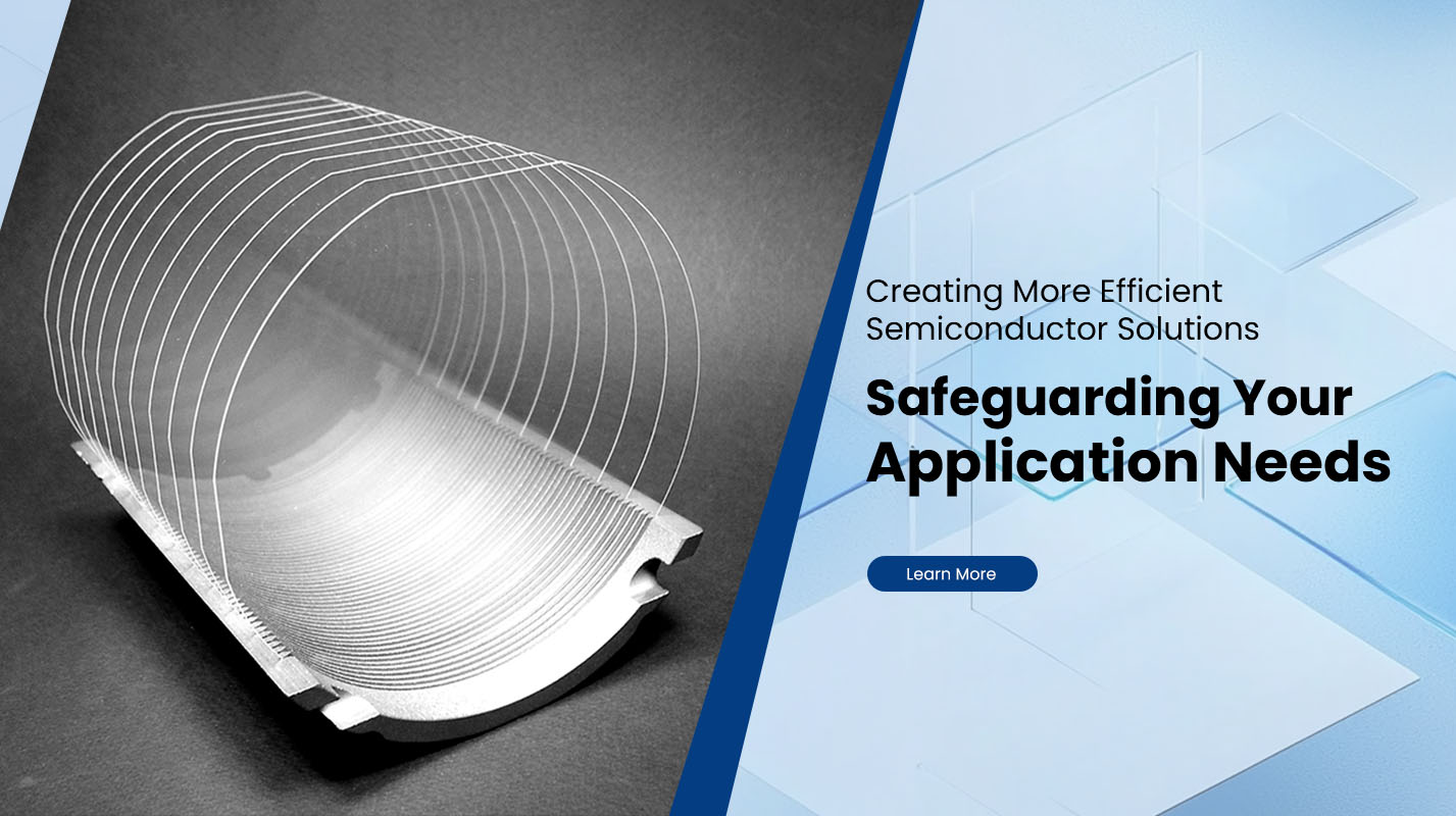
What Are Compound Semiconductor Wafers?
Compound Semiconductor Wafers are single-crystal substrates made from two or more elements rather than elemental silicon. They serve as the “starting platform” for building devices where silicon can struggle, such as high-power switching, high-frequency RF, optoelectronics, or advanced sensing. In practical manufacturing terms, a compound wafer is the mechanically stable, crystallographically aligned base on which you grow epitaxial layers, deposit films, pattern circuits, and finally singulate into dies.
Unlike mainstream silicon, compound materials span multiple crystal families and growth methods, so wafer selection is less about a single standard and more about matching material system + crystal quality + surface condition to the device roadmap. PLUTOSEMI supplies a broad range of compound semiconductor wafers, including SiC, GaAs, GaN substrates, Ga2O3, InP, InSb, InAs, and functional oxide substrates such as SrTiO3, plus optical-grade LiNbO3 and LiTaO3 options.
Why Compound Wafers Matter in Device Performance
A wafer’s intrinsic material properties determine the ceiling of what a device can do:
Wide-bandgap platforms support higher breakdown fields and higher temperature operation, making them attractive when power density and thermal margin matter.
III–V substrates are favored when you need high electron mobility, efficient light emission, or high-frequency performance.
Specialty functional crystals enable electro-optic or piezoelectric behaviors used in advanced photonics and acoustic-wave devices.
Because these materials are often used at the edge of performance, wafer quality is directly tied to yield and reliability. Small differences in defects, polish, or geometry can show up later as leakage, premature breakdown, film stress, or lithography issues.
Main Types of Compound Semiconductor Wafers
Below is a practical “selection map” of common compound substrates and what typically drives their adoption. (Specific device design should be validated with your process team.)
| Wafer type | What it is | Typical decision driver |
|---|---|---|
| SiC (Silicon Carbide) | Wide-bandgap single crystal | High-voltage, high-temperature, high-power capability |
| GaN substrate | Nitride wide-bandgap crystal | High-power RF and power devices requiring strong material performance |
| GaAs (Gallium Arsenide) | III–V compound crystal | High-frequency RF and optoelectronic performance needs |
| InP (Indium Phosphide) | III–V compound crystal | High-speed photonics and advanced communication components |
| InAs / InSb | Narrow-gap III–V crystals | Infrared-related sensing and specialized electronics requirements |
| Ga2O3 (Gallium Oxide) | Ultra-wide-bandgap oxide | Emerging high-breakdown applications and R&D exploration |
| SrTiO3 | Single-crystal oxide substrate | Functional oxide films and advanced materials research |
| LiNbO3 / LiTaO3 | Optical-grade functional crystals | Electro-optic and acoustic-wave related platforms |
PLUTOSEMI lists these compound categories as part of its product portfolio, helping teams source the right substrate family early in a program. :contentReference[oaicite:1]{index=1}
Key Specs Buyers Should Lock Before Quoting
When sourcing compound wafers, the fastest way to reduce back-and-forth is to define the technical “must-haves” up front. These parameters influence process stability and cost:
1) Size and thickness window
Confirm target diameter and thickness range based on tool compatibility, handling, and warp tolerance.
2) Crystal orientation and off-cut
Orientation affects epitaxial behavior, etch characteristics, and device performance. Off-cut choices can be process-critical for certain epitaxy stacks.
3) Doping type and resistivity targets
Define conductivity type and target resistivity range to align with device layers and electrical isolation strategy.
4) Surface finish and roughness expectation
Specify polish type and surface quality needs. For many fabs, this is where lithography stability and film uniformity begin.
5) Geometry controls
Agree on TTV, bow, and warp limits so your line can stay within focus budgets and chucking limits.
6) Quality/inspection requirements
Align on inspection methods and acceptance criteria suitable for your stage: prototyping, pilot, or volume.
If you run multi-node programs, consider standardizing a “core spec template” so different wafer types can be quoted consistently across projects and bulk order planning.
How PLUTOSEMI Supports Manufacturing Programs
From a manufacturer-and-supplier perspective, the goal is not just to ship wafers, but to make your downstream process predictable. PLUTOSEMI positions itself as a high-performance semiconductor materials supplier with broad product coverage across wafer categories, and also provides process-oriented services such as epitaxial-related offerings and wafer foundry support to help teams reduce supplier fragmentation.
Operationally, PLUTOSEMI also highlights multi-base production capacity designed for stable supply, which is especially important when you are moving from sampling into sustained demand.
For programs needing customization, PLUTOSEMI emphasizes tailored solutions, which can be valuable for OEM/ODM-style development where specs evolve across engineering builds.
A Simple Sourcing Workflow That Reduces Risk
Freeze the “non-negotiables”: diameter, orientation/off-cut, conductivity type, surface finish.
Set geometry targets: TTV, bow/warp, edge profile expectations.
Define inspection scope by phase: R&D vs pilot vs production.
Plan continuity: if scaling, confirm how the same spec will be maintained across repeat lots.
Keep a change log: document every spec revision so engineering, purchasing, and production stay aligned.
Done well, this turns wafer sourcing from a reactive task into a controllable input to yield and reliability.
Closing Note
Compound semiconductor wafers unlock performance regimes that silicon cannot easily reach, but they demand tighter alignment between material choice, wafer specification, and process flow. If you share your target device direction and tool constraints, PLUTOSEMI can help map the appropriate wafer family and define a spec package that supports repeatable fabrication and scalable supply. :contentReference[oaicite:5]{index=5}


