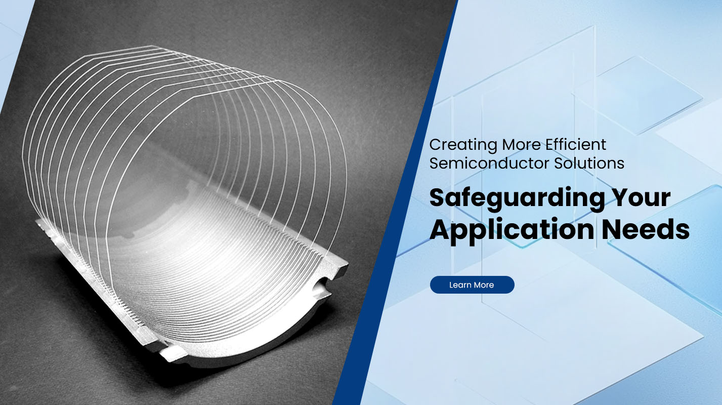
How It's Made Silicon Wafer?
As a manufacturer of Silicon Wafers, we're often asked about the fascinating process that transforms raw sand into the ultra-pure, mirror-like discs powering all modern electronics. Here's an in-depth look at how we create the foundation of the semiconductor industry.
Stage 1: From Sand to Semiconductor-Grade Silicon
1.1 Silicon Purification
The journey begins with ordinary quartzite sand (SiO₂) mined from select locations worldwide. Through a multistep refinement process:
Carbothermic Reduction: Sand is mixed with carbon and heated to 2000°C in arc furnaces, producing 98% pure metallurgical-grade silicon (MGS)
Hydrochlorination: MGS reacts with hydrogen chloride to form trichlorosilane (HSiCl₃)
Distillation: Multiple distillation towers remove impurities like boron and phosphorus
Siemens Process: High-purity trichlorosilane is decomposed at 1100°C onto ultra-pure silicon rods, creating electronic-grade silicon (EGS) with 99.9999999% purity ("9N")
1.2 Ingot Growth
Two primary methods create single-crystal silicon ingots:
Czochralski (CZ) Method (80% of wafers)
EGS is melted in quartz crucibles at 1420°C
A seed crystal is dipped into the melt and slowly pulled (1-100mm/min) while rotating
Precise control of temperature gradients creates perfect single crystals
Doping occurs by adding precise amounts of boron (p-type) or phosphorus (n-type)
Float Zone (FZ) Method (for high-resistivity wafers)
A polycrystalline rod is zone-refined using RF heating
Produces crystals with lower oxygen content than CZ
Stage 2: Ingot Processing
2.1 Diameter Standardization
Ingots are ground to exact diameters:
150mm (6"), 200mm (8"), 300mm (12") - with 450mm in development
Our laser measurement systems maintain ±0.1mm tolerance
2.2 Orientation Flats/Notches
Primary flat indicates crystal orientation (typically <110>)
Secondary flat denotes doping type
On 300mm wafers, notches replace flats for space efficiency
2.3 Resistivity Testing
Four-point probe measurements verify:
p-type: 1-100 ohm-cm
n-type: 0.001-100 ohm-cm
Stage 3: Wafer Slicing
3.1 Wire Saw Technology
Diamond-coated wires (0.1mm diameter) in slurry cut 300+ wafers simultaneously
Cutting speeds up to 2mm/min with <25µm thickness variation
Kerf loss reduced to 150µm through advanced wire guides
3.2 Edge Grinding
Precision grinding creates rounded edges to:
Prevent chipping
Reduce stress concentrations
Improve photoresist coating uniformity
Stage 4: Surface Preparation
4.1 Lapping & Etching
Double-side lapping achieves <1µm flatness
Acidic (HNO₃/HF) or alkaline (KOH) etching removes 20-50µm of damaged silicon
4.2 Polishing
Chemical-mechanical planarization (CMP) using:
Colloidal silica slurry (pH 10-11)
Polyurethane polishing pads
Downforce of 3-7 psi
Achieves surface roughness <0.2nm RMS
4.3 Cleaning
SC1/SC2 RCA cleaning removes:
Organic contaminants (H₂O₂/NH₄OH)
Metallic impurities (H₂O₂/HCl)
Particles down to <10/nm @ 45nm size
Stage 5: Metrology & Packaging
5.1 Quality Control
Thickness: Laser gauges measure to ±0.25µm
Flatness: Capacitive sensors detect <0.3µm TTV
Surface defects: Dark-field scanners detect >0.12µm particles
Crystal defects: X-ray topography identifies dislocations
5.2 Packaging
Class 1 cleanroom environment
Vacuum-sealed cassettes with nitrogen purge
Shipping containers with <1 PPM oxygen
Technical Specifications Comparison
| Parameter | 150mm Wafer | 200mm Wafer | 300mm Wafer |
|---|---|---|---|
| Thickness | 675µm | 725µm | 775µm |
| Weight | 27g | 53g | 128g |
| Die/wafer* | 200 | 450 | 1,300 |
| Bow/Warp | <50µm | <60µm | <70µm |
(*for typical 10mm² die)
Future Innovations
Our R&D focuses on:
450mm wafer transition (40% more die/wafer)
Epitaxial growth with <0.5% thickness variation
SOI wafers with 25nm buried oxide layers
Patterned wafers with embedded nanostructures
Silicon wafers remain the most precisely engineered materials in human history - with over 200 controlled parameters in their manufacture. As we push toward atomic-level perfection, these crystalline foundations will continue enabling smaller, faster, and more efficient electronics for decades to come.


