

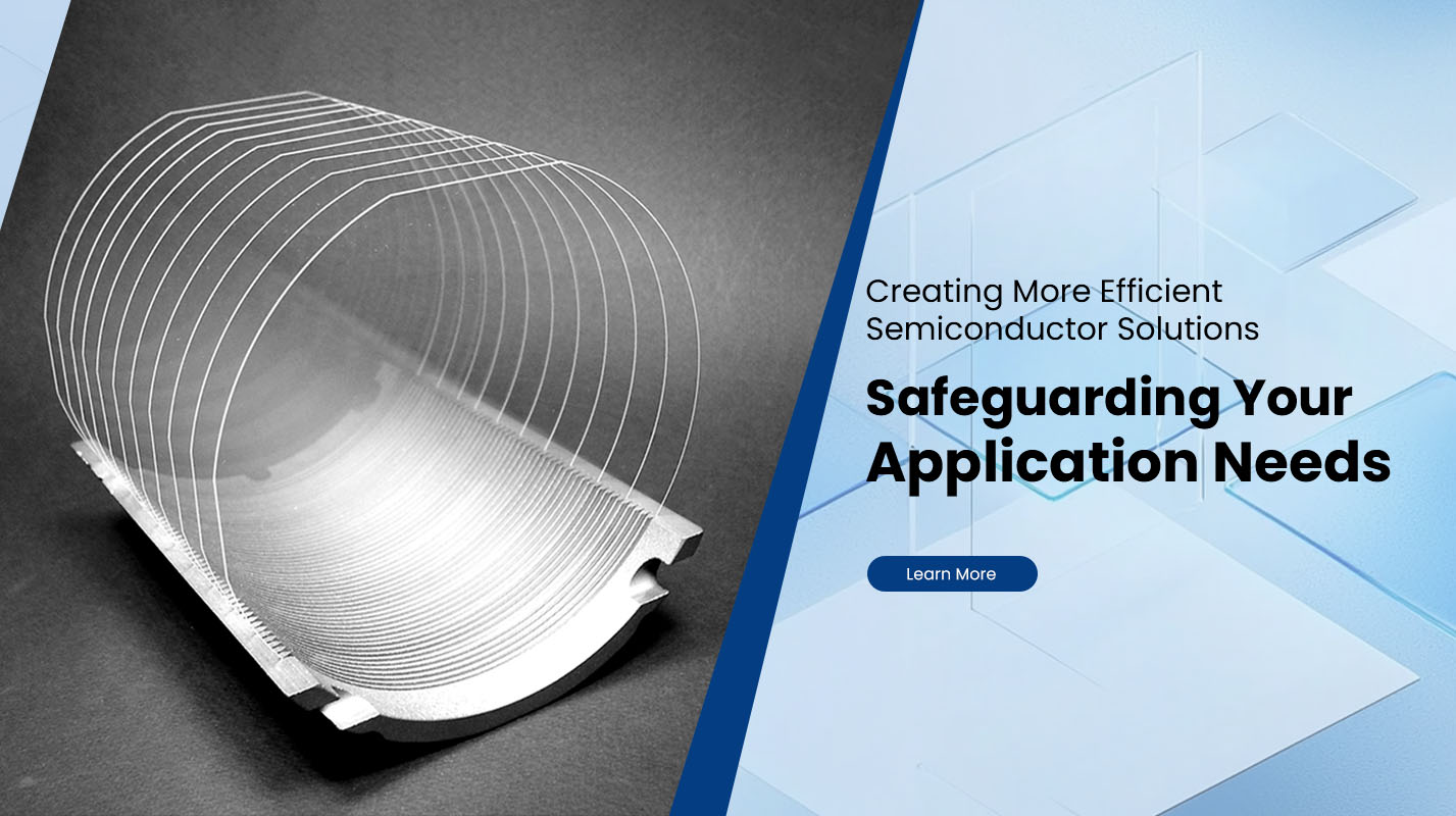
How Many Dies Can Be Produced from One Silicon Wafer?
A Silicon Wafer can produce dozens to thousands of dies, depending on wafer diameter, die footprint, edge exclusion, and yield. For a 300 mm wafer with a 10 × 10 mm die footprint, a common geometric estimate is about 614 gross dies before defect-related losses.
What Determines the Number of Dies per Wafer?
The number of dies per wafer, also called dies per wafer or die count per wafer, depends primarily on the usable wafer area and the footprint of each die.
Four factors are especially important:
Wafer diameter: Larger wafers provide more usable area, allowing more dies to fit when the die design and process requirements remain comparable.
Die size: Smaller dies generally allow more units to fit on a wafer. However, the final count also depends on the die's rectangular dimensions and layout.
Edge exclusion: The outer edge of a wafer may be unsuitable for placing complete dies because of process, handling, or design constraints.
Scribe lanes and layout rules: Small gaps between dies are required for separation, while reticle limits and alignment structures can further affect the usable layout.
The theoretical wafer area divided by die area provides an initial upper bound. A more practical estimate must account for dies that cannot fit completely within the circular wafer boundary.
How Do You Calculate Dies per Wafer?
A commonly used first-order approximation for gross dies per wafer is:
Gross dies per wafer ≈ (π × D² / 4A) − (π × D / √(2A))
Where:
D is the effective wafer diameter after edge exclusion, measured in millimeters.
A is the die footprint area in square millimeters, including the allocated scribe-lane space.
π is approximately 3.1416.
The first term estimates how many die footprints could fit based on wafer area. The second term approximates the loss of complete dies around the circular edge.
This formula is useful for early engineering estimates, but it is not an exact die-layout calculation. Die aspect ratio, scribe-lane dimensions, edge rules, and actual layout constraints can change the result.
How Many Dies Fit on a 300 mm Silicon Wafer?
Consider a 300 mm silicon wafer with a 3 mm edge exclusion on each side. The effective diameter is 294 mm.
Assuming square die footprints that already include scribe-lane space, the approximate gross die counts are:
| Die footprint | Approximate gross dies per wafer |
|---|---|
| 5 × 5 mm | 2,584 |
| 10 × 10 mm | 614 |
| 20 × 20 mm | 137 |
These figures are illustrative estimates rather than guaranteed production counts. The actual number depends on the die layout, edge exclusion, and applicable manufacturing rules.
The comparison also shows why wafer diameter alone is insufficient for estimating output. A smaller die footprint can substantially increase the number of dies per wafer, while larger dies leave fewer complete units around the wafer's perimeter.
How Does Die Yield Affect the Number of Usable Chips?
Gross dies per wafer and good dies per wafer are different measurements.
Gross die count represents the estimated number of complete die footprints that fit on the wafer. Good die count represents the number of dies that meet the required functional and electrical specifications after the relevant manufacturing and testing stages.
A simplified calculation is:
Estimated good dies per wafer = Gross dies per wafer × Die yield
For example, if a wafer contains an estimated 614 gross dies and the actual die yield is 90%, the expected number of good dies is approximately 553.
The 90% yield in this example is hypothetical, not a universal semiconductor industry benchmark.
Actual yield depends on defect density, die area, process maturity, material quality, electrical performance requirements, and other manufacturing factors. Larger dies can be more sensitive to random defects because a greater area is exposed to potential defect-related failures.
For production planning, gross die count should therefore be evaluated alongside expected yield rather than treated as the final number of deliverable chips.
Does Wafer Quality Affect Die Count and Manufacturing Efficiency?
Wafer quality can influence how consistently a wafer moves through subsequent manufacturing processes. Important specifications include thickness variation, flatness, surface condition, particle contamination, and dimensional tolerances.
These parameters do not directly determine the geometric die count in the same way as wafer diameter and die footprint. However, they can affect process stability, defect risk, and the proportion of dies that meet the required specifications.
For applications involving precision lithography, wafer bonding, or other processes with tight geometric tolerances, an appropriately specified Ultra Flat Silicon Wafers may be relevant. For general semiconductor substrate requirements, a Mirror Polished Silicon Wafer may be considered according to the required diameter, thickness, orientation, resistivity, and surface finish.
Product selection should be based on the intended process and confirmed specifications rather than assuming that a higher flatness specification automatically increases the number of dies per wafer.
How Can Buyers Estimate Die Output Before Selecting a Wafer?
Before comparing wafer specifications or estimating production costs, buyers and engineering teams should confirm the following information:
Wafer diameter: Identify the nominal diameter and applicable edge exclusion.
Die dimensions: Provide the die width and height, rather than only the active circuit area.
Scribe-lane requirements: Include the spacing allocated between adjacent dies.
Layout constraints: Consider reticle field limits, alignment structures, and other applicable design rules.
Expected yield: Use process-specific yield data to estimate the number of functional dies.
Quality requirements: Confirm wafer specifications and acceptance criteria that may influence downstream processing.
For early-stage planning, a gross die calculation is sufficient to compare alternative wafer sizes or die footprints. Before committing to production quantities or cost estimates, the result should be validated against the actual die layout and manufacturing process.
PLUTOSEMI provides a range of silicon wafer products for different semiconductor material and processing requirements. Buyers can review the available specifications and submit their wafer diameter, thickness, surface finish, and application requirements for further evaluation.