

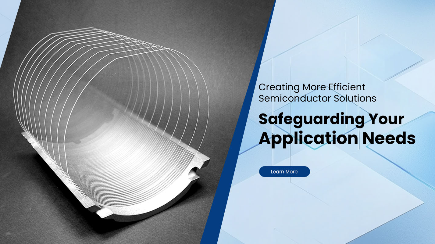
What Is the Difference Between Ultra-Flat and Standard Silicon Wafers for Precision Processing?
Ultra-flat Silicon Wafers offer tighter control of thickness variation, wafer geometry, and surface consistency than standard wafers specified for less demanding processes. They are most useful when lithography, wafer bonding, thinning, or precision alignment requires a narrower process window.
What Is an Ultra-Flat Silicon Wafer?
An ultra-flat silicon wafer is a silicon substrate manufactured to meet demanding geometric specifications, particularly for total thickness variation (TTV), flatness, and surface parallelism. Compared with a standard wafer that meets general application requirements, an ultra-flat wafer is designed for processes where small geometric deviations can affect equipment contact, alignment, or processing consistency.
The term ultra-flat does not represent one universal tolerance applicable to every wafer diameter and thickness. Actual performance depends on the substrate dimensions, polishing method, measurement conditions, and agreed acceptance criteria.
For example, PLUTOSEMI lists its Ultra Flat Silicon Wafers with 4-inch and 6-inch diameter options, thicknesses from 200 to 1,500 μm, and a specified TTV limit of 2 μm, with actual values stated as reaching 1 μm or below. These specifications illustrate the importance of evaluating measurable parameters rather than relying on the product name alone.
How Do Ultra-Flat and Standard Silicon Wafers Compare?
The main difference is the level of geometric control required by the downstream process.
| Evaluation factor | Standard Silicon Wafer | Ultra-Flat Silicon Wafer |
|---|---|---|
| Thickness variation | Meets the specified tolerance for the intended application | Designed for tighter thickness consistency |
| Wafer geometry | Depends on the selected grade and manufacturing specification | Emphasizes controlled flatness and deformation |
| Surface parallelism | Depends on wafer processing and acceptance criteria | Often a key requirement for precision applications |
| Polishing method | Single-side or double-side processing, depending on requirements | Double-side precision grinding and polishing may be used |
| Lithography | Suitable when the wafer meets the tool's focus and geometry limits | Useful when geometry control is especially demanding |
| Wafer bonding | Suitable when surface contact and geometry requirements are met | Can help reduce geometric variation affecting bonding contact |
| Cost considerations | May be more economical when standard tolerances are sufficient | Tighter processing and inspection requirements may increase cost |
| Typical selection priority | General process compatibility and cost efficiency | Repeatability and tighter geometric tolerances |
A standard wafer is not necessarily unsuitable for precision processing. Some standard-grade wafers already meet demanding requirements, while some applications may not benefit from tighter tolerances. The correct comparison must use actual specifications for both options.
What Is the Difference Between TTV, Flatness, Bow, and Warp?
These parameters describe different aspects of wafer geometry. Understanding them is essential when deciding whether an ultra-flat wafer is necessary.
Total Thickness Variation (TTV) is the difference between the maximum and minimum measured wafer thickness across the defined measurement area. Lower TTV indicates more consistent thickness, which can be important for uniform processing and bonding.
Flatness describes how closely a wafer surface conforms to a defined reference plane under specified measurement conditions. Global flatness and local or site flatness can describe different areas and scales of surface variation.
Bow describes the overall curvature of a wafer in its free, unclamped state. Excessive bow can affect how the wafer contacts a vacuum chuck or another processing surface.
Warp describes the overall out-of-plane shape variation of a wafer. Unlike bow, which characterizes a particular curvature measure, warp can capture more complex deformation across the wafer.
These measurements should not be used interchangeably. A wafer can have low TTV but still exhibit excessive bow or warp. Similarly, a wafer with acceptable overall geometry may not meet the local flatness requirement of a sensitive lithography process.
For precision procurement, the specification should identify the required metrics, their maximum limits, the measurement method, and the applicable edge exclusion.
When Should You Choose an Ultra-Flat Silicon Wafer for Lithography?
Lithography transfers patterns onto a wafer surface using tightly controlled alignment and focusing. Variations in wafer geometry can affect the position of the surface relative to the exposure system, potentially reducing focus margin or increasing pattern variation.
An ultra-flat wafer can be useful when the process requires consistent surface positioning across exposure sites, particularly when the equipment has strict geometry limits.
However, wafer flatness alone does not determine lithography performance. Resist thickness, surface cleanliness, chucking behavior, exposure conditions, and equipment calibration also influence the final result.
Before selecting a wafer, confirm the required global and local flatness, TTV, bow, warp, and wafer thickness. The tightest requirement should be based on the actual tool and process window rather than an assumption that the lowest available TTV is always necessary.
Are Ultra-Flat Silicon Wafers Better for Wafer Bonding?
Ultra-flat wafers can be advantageous in bonding processes because geometric variation may affect the contact between two substrates. Bow, warp, local surface variation, and thickness differences can contribute to incomplete contact or nonuniform bonding conditions.
For applications involving direct bonding or precision substrate stacking, both wafer geometry and surface condition matter. Surface roughness, particles, cleanliness, material compatibility, and the bonding method must be considered alongside flatness.
Double-side polished ultra-flat wafers may be appropriate when both surfaces require controlled finishing or when parallelism is important to the bonding structure. Nevertheless, double-side polishing does not automatically guarantee successful bonding. The surfaces must still satisfy the requirements of the selected bonding process.
When specifying wafers for bonding, buyers should identify the bonding method, substrate thickness, required TTV, bow and warp limits, surface roughness, and cleanliness criteria.
How Does Wafer Thickness Affect Flatness Requirements?
Wafer thickness influences mechanical rigidity and the wafer's response to handling, processing forces, and residual stress. Thinner wafers generally deform more easily than thicker wafers of comparable diameter and material under similar conditions.
This becomes important during back grinding, thinning, precision dicing, and wafer transfer. Geometric variation that is manageable in a thicker substrate may create handling or process-control challenges when the substrate becomes thinner.
For applications requiring thin substrates, an Ultra Thin Silicon Wafer may be relevant, but thickness and flatness should be evaluated separately. A thin wafer does not automatically have ultra-flat geometry, and an ultra-flat wafer is not necessarily intended for every thin-wafer application.
The purchase specification should therefore define nominal thickness, TTV, bow, warp, and any support or handling requirements. If the wafer will undergo further thinning or film deposition, the expected changes in geometry should also be considered.
How Should Buyers Specify Ultra-Flat Silicon Wafers?
A useful procurement specification translates the requirements of the downstream process into measurable acceptance criteria.
Before requesting a quotation, confirm the following:
Wafer dimensions: Specify the diameter, nominal thickness, and dimensional tolerances.
Thickness uniformity: Define the maximum TTV and the measurement area.
Wafer geometry: State the required bow, warp, and flatness limits where applicable.
Surface finish: Specify single-side or double-side polishing and the required surface roughness.
Cleanliness: Define particle limits, contamination requirements, and inspection conditions.
Application requirements: Identify whether the wafer will be used for lithography, bonding, thinning, dicing, or another precision process.
Inspection and consistency: Confirm the measurement method, reporting format, sampling plan, and lot-to-lot acceptance criteria.
These details help suppliers determine whether a standard wafer already meets the process requirements or whether an ultra-flat specification is justified.
For repeated production orders, evaluating multiple wafers from a sample lot can also help establish whether the supplier's geometry control is sufficiently consistent. A single conforming wafer does not necessarily demonstrate consistent performance across future batches.
How Can You Avoid Paying for Unnecessary Flatness?
The most effective approach is to select the wafer according to the most demanding step in the actual process sequence.
If standard wafers consistently meet the equipment limits and process requirements, upgrading to an ultra-flat grade may not provide enough benefit to justify the additional cost. Conversely, if wafer geometry repeatedly affects bonding, lithography, or thinning stability, tighter incoming specifications may reduce process adjustments and material losses.
A practical evaluation compares three factors:
Process sensitivity: Identify which geometric deviations can cause defects or equipment problems.
Specification capability: Confirm that the proposed wafer meets the required limits with appropriate inspection evidence.
Total process cost: Consider the cost of the substrate alongside rework, scrap, equipment adjustments, and production variability.
The objective is not to purchase the flattest possible wafer in every case. It is to purchase the least restrictive specification that reliably meets the manufacturing requirements.
Which Silicon Wafer Products Should You Consider?
For general semiconductor applications, a Mirror Polished Silicon Wafer may be suitable when the specified surface finish and geometry meet the requirements of the process.
For applications requiring tighter geometric control, PLUTOSEMI's Ultra Flat Silicon Wafers are worth evaluating for their double-side polished configuration and specified thickness-uniformity requirements.
Product selection should be based on confirmed wafer specifications rather than the distinction between standard and ultra-flat labels alone. Buyers should compare TTV, bow, warp, surface finish, particle limits, and measurement conditions before selecting a substrate.
When requesting a quotation, provide the intended application, wafer diameter, thickness, target geometric tolerances, and required inspection documentation. This allows the proposed specification to be evaluated against the actual process window.
Final Recommendation: Is an Ultra-Flat Silicon Wafer Worth the Upgrade?
An ultra-flat silicon wafer is worth considering when tight geometric control is essential for lithography, wafer bonding, thinning, or other precision operations. Standard silicon wafers remain appropriate when their verified specifications already satisfy the required process limits.
The best choice depends on the interaction between wafer geometry, surface condition, equipment capability, and downstream processing. Comparing measurable tolerances and lot consistency provides a more reliable purchasing decision than choosing a wafer based on its grade name alone.