How Thick Is A Silicon Wafer?
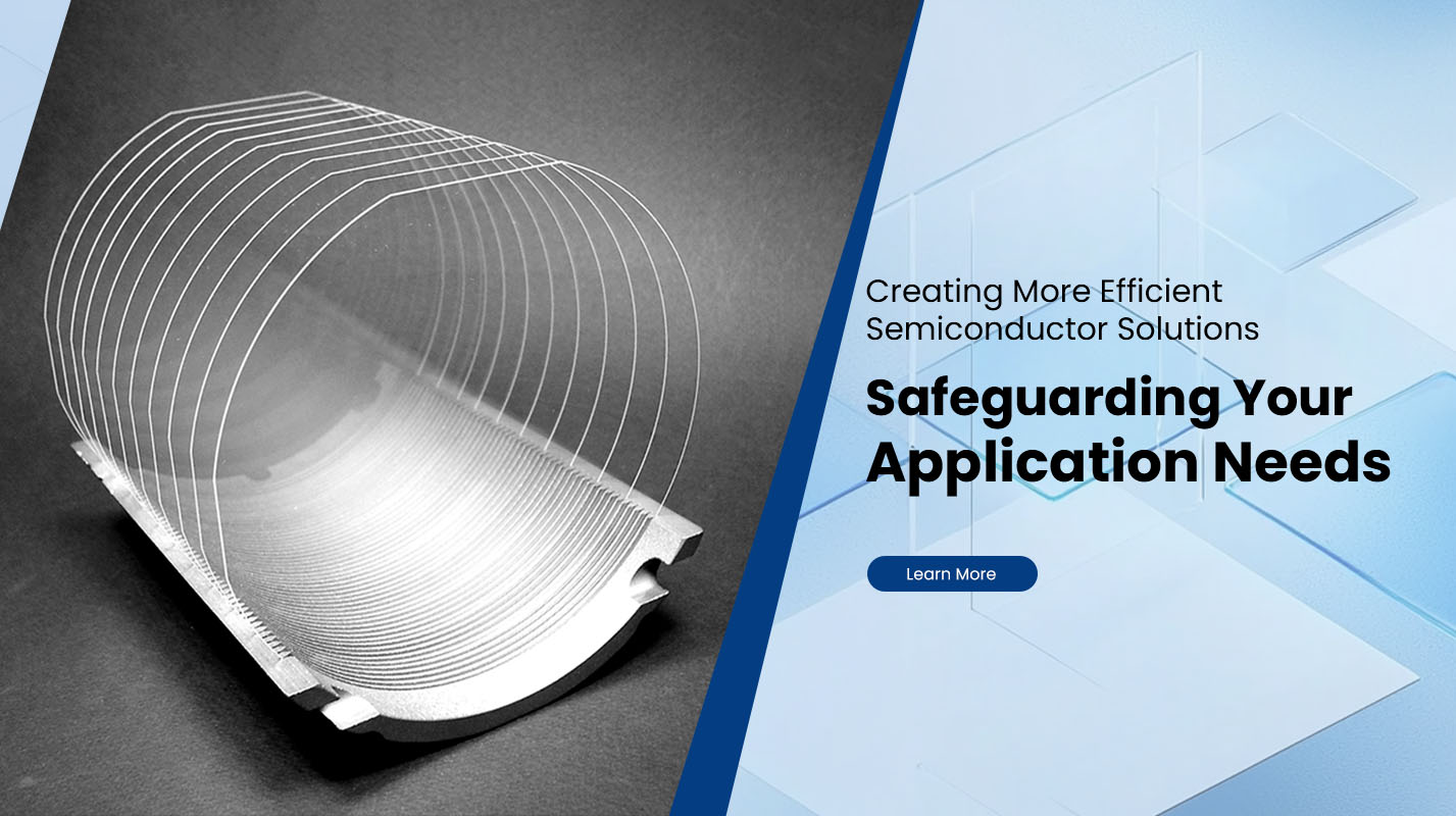
Silicon Wafers are the foundation of modern electronics. They are thin slices of semiconductor material, primarily silicon, used in the fabrication of integrated circuits (ICs) and microchips. The thickness of a silicon wafer is a critical parameter that affects its performance, durability, and application. In this article, we will explore the typical thickness of silicon wafers, the factors that influence their thickness, and the importance of precise thickness control in semiconductor manufacturing.
Typical Thickness of Silicon Wafers
The thickness of a silicon wafer can vary significantly depending on its intended use and the manufacturing process. Generally, silicon wafers used in semiconductor manufacturing range from a few hundred micrometers to a few millimeters in thickness. Here are some common thickness ranges for different types of silicon wafers:
Standard Wafers
200 mm (8-inch) Wafers: Typically, these wafers have a thickness of around 675 micrometers (µm) to 725 µm.
300 mm (12-inch) Wafers: These larger wafers usually have a thickness of approximately 775 µm to 825 µm.
Thinner Wafers
MEMS (Micro-Electro-Mechanical Systems) Wafers: These specialized wafers can be as thin as 50 µm to 100 µm, depending on the specific MEMS device being fabricated.
Flexible Electronics Wafers: For applications requiring flexibility, such as wearable devices, the wafer thickness can be reduced to as low as 20 µm to 50 µm.
Thicker Wafers
Power Electronics Wafers: In applications like power modules, where higher current handling and thermal management are required, the wafer thickness can be up to 1 mm or more.
Factors Influencing Wafer Thickness
Several factors determine the thickness of a silicon wafer:
Application Requirements
Integrated Circuits: For standard ICs, the thickness is optimized to balance mechanical strength and electrical performance. Thinner wafers can reduce parasitic capacitance and improve performance but may be more fragile.
Power Devices: Thicker wafers are often used for power devices to handle higher currents and dissipate heat more effectively.
MEMS Devices: The thickness is tailored to the specific mechanical properties required for the MEMS structure, such as sensors or actuators.
Manufacturing Process
Crystal Growth: The initial thickness is determined during the crystal growth process. The Czochralski (CZ) or Float Zone (FZ) methods are commonly used to grow silicon ingots, which are then sliced into wafers.
Slicing and Polishing: The slicing process uses diamond saws to cut the ingot into wafers. The thickness can be adjusted during this step. Subsequent polishing steps can also slightly reduce the thickness.
Thermal and Mechanical Considerations
Thermal Management: Thicker wafers can better dissipate heat, which is crucial for high-power applications.
Mechanical Strength: Thicker wafers are more robust and less prone to breakage during handling and processing.
Importance of Precise Thickness Control
Precise control of wafer thickness is essential for several reasons:
Electrical Performance
Reduced Parasitics: Thinner wafers can reduce parasitic capacitance and resistance, leading to higher performance in high-speed and high-frequency applications.
Uniformity: Uniform thickness ensures consistent electrical properties across the wafer, which is critical for the reliability and performance of the final devices.
Manufacturing Yield
Higher Yield: Consistent thickness reduces the likelihood of defects during processing, such as cracking or warping, which can improve manufacturing yield.
Cost Efficiency: Accurate thickness control can minimize material waste and reduce production costs.
Device Integration
Stacking and Packaging: In advanced packaging techniques, such as 3D stacking, precise thickness control is necessary to ensure proper alignment and integration of multiple wafers.
Techniques for Measuring Wafer Thickness
Accurate measurement of wafer thickness is crucial in semiconductor manufacturing. Several techniques are used to measure the thickness of silicon wafers:
Contact Measurement
Micrometers: Mechanical micrometers can be used to measure the thickness of wafers. However, this method can be destructive and is not suitable for high-precision measurements.
Non-Contact Measurement
Optical Interferometry: This technique uses light interference patterns to measure the thickness with high precision. It is non-destructive and can provide accurate measurements at the nanometer level.
Laser Triangulation: A laser is projected onto the wafer surface, and the reflected light is used to determine the thickness. This method is also non-destructive and can measure thickness with high accuracy.
Future Trends in Wafer Thickness
As technology advances, the trend is towards thinner wafers for many applications:
Moore's Law and Miniaturization
Smaller Devices: As transistors and other components continue to shrink, the demand for thinner wafers increases to accommodate more devices per wafer and improve performance.
3D Integration: The development of 3D integrated circuits (3D ICs) requires thinner wafers to enable stacking and interconnection of multiple layers.
Emerging Applications
Flexible Electronics: The growth of flexible and wearable electronics necessitates thinner wafers that can be bent or folded without breaking.
Advanced Packaging: Techniques like through-silicon vias (TSVs) and fan-out wafer-level packaging (FOWLP) benefit from thinner wafers to achieve higher integration density and performance.
Previous: What Is SOI?


