What Is A Silicon Wafer Used for?
Silicon Wafers are fundamental to modern electronics. From smartphones to sensors, they provide the base (substrate) that makes semiconductor devices, MEMS, power systems, and photonics possible. This article explains what silicon wafers are, their special variants like SOI (Silicon-on-Insulator), and where & how they are used. We also describe how companies like Plutosemi deliver advanced wafers meeting high-precision demands for diverse applications.
What Is a Silicon Wafer
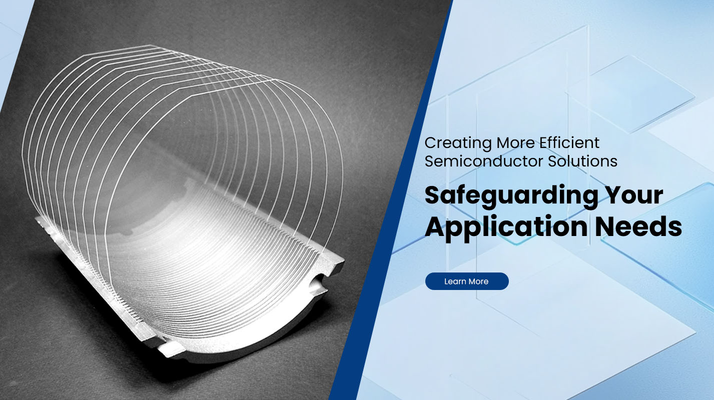
A silicon wafer is a thin, flat disc of highly pure, single-crystalline or polycrystalline silicon. It is polished to a mirror-like surface, with extremely low roughness and minimal defects, so that microfabrication (lithography, etching, doping, etc.) can occur reliably.
Key properties include:
High purity (often “electronic‐grade” silicon) to prevent unwanted electrical behavior.
Uniform crystal structure so that electrical behavior is predictable.
Surface flatness and cleanliness—imperfections or contaminants degrade performance.
What Is SOI (Silicon-on-Insulator)
One important variant is SOI wafers: these consist of a thin device layer of silicon separated from the bulk substrate by an insulating layer (usually silicon dioxide). The “buried oxide” (BOX) layer improves electrical isolation and helps reduce parasitic capacitances, leakage currents, and power consumption.
SOI’s advantages include:
Better performance in high-frequency / RF circuits.
Lower power usage (especially important for mobile, IoT).
Improved performance in MEMS, sensors, photonics, etc. because of mechanical stability or optical confinement.
Applications of Silicon Wafers & SOI
Here are the main application areas where silicon wafers (and SOI wafers) are used:
| Application Area | What They Do / Why A Wafer Is Needed | Role of SOI Variant, If Any |
|---|---|---|
| Integrated Circuits (ICs) / Microprocessors / Memory chips | Silicon wafers are the substrate on which billions of transistors are fabricated using photolithography, doping, deposition, etc. Without a high-quality wafer, defects, leakage, and yield issues arise. | SOI enhances performance by reducing parasitic effects, improving speed, and lowering power consumption. |
| Radio Frequency (RF) Devices / 5G / Communication Chips | High-frequency circuits need better isolation and lower noise; substrate properties are critical. | SOI enables better isolation, lower parasitic capacitances, improving RF performance. |
| Sensors, MEMS (Micro-Electro-Mechanical Systems) | Applications like accelerometers, gyroscopes, pressure sensors, micro-mirrors etc. need precise mechanical stability, well-controlled layers, etc. | SOI wafers are preferred for many MEMS because the thin top silicon layer over insulating oxide gives defined device layers and etch stop layers. |
| Photonics & Optoelectronics | Devices that guide, modulate, emit or detect light (e.g. optical waveguides, photonic integrated circuits, LiDAR) benefit greatly from substrates with optical confinement and clean interfaces. | SOI wafers are heavily used in photonics, since the buried oxide layer confines light and reduces loss. |
| Power Electronics | Devices that handle high voltages / currents need substrates that can withstand heat and have low leakage. | SOI can help for certain power devices; also different types of bulk wafers are used, sometimes special high-resistivity or engineered substrates. |
| Solar Cells & Photovoltaics | In solar panels, silicon wafers are used to make the p-n junction that converts light into electricity. Although Solar Wafers can have different purity or thickness requirements compared to IC wafers. |
Why Precision, Quality & Customization Matter
Because the technologies built on wafers are so small and complex:
Even minor defects or impurities can lead to large failures (yield, overheating, leakage).
Thickness, flatness, doping, resistivity, crystal orientation all must be tightly controlled.
Specialized adaptations (like SOI, or specific device layers, or patterned or bonded wafers) are needed for advanced designs.
Plutosemi & Our Role
At Plutosemi, we specialize in providing high-quality silicon wafers and SOI wafers with advanced production capabilities. Key points about us:
We focus on high precision in wafer thickness, flatness, and surface quality, to serve demanding applications.
Our product range covers both bulk silicon wafers and SOI substrates, enabling electronic, RF, photonic, MEMS, and power applications.
Our customers rely on us for wafers that meet stringent specifications, helping engineers and designers build reliable, high-performance devices.
Future Trends
Looking ahead, some of the trends and challenges include:
Scaling to smaller nodes: as transistor sizes shrink, substrate & SOI quality requirements tighten.
3D integration & stacked dies: wafer‐level thinning, bonding can require new substrate formats and tolerances.
Energy efficiency: low-power/ultra-low leakage SOI devices for IoT and wearable devices.
Photonics convergence: integrating photonic components (light emission, detection, guiding) onto silicon platforms, often using SOI wafers.
Diverse semiconductor materials: while silicon dominates, hybrid systems (e.g. silicon + III-V materials, or silicon carbide) are growing in power / optoelectronic sectors.
Summary
Silicon wafers are the foundational substrate for most semiconductor devices. SOI wafers add insulating layers for enhanced performance. Their applications span ICs, RF, MEMS, photonics, power electronics, and solar. High quality, high precision, and appropriate customization are essential for modern technologies—and companies like Plutosemi help deliver wafers that meet those demanding requirements.
Previous: Why Silicon Wafer Is Circular?
Next: What Is SOI?


