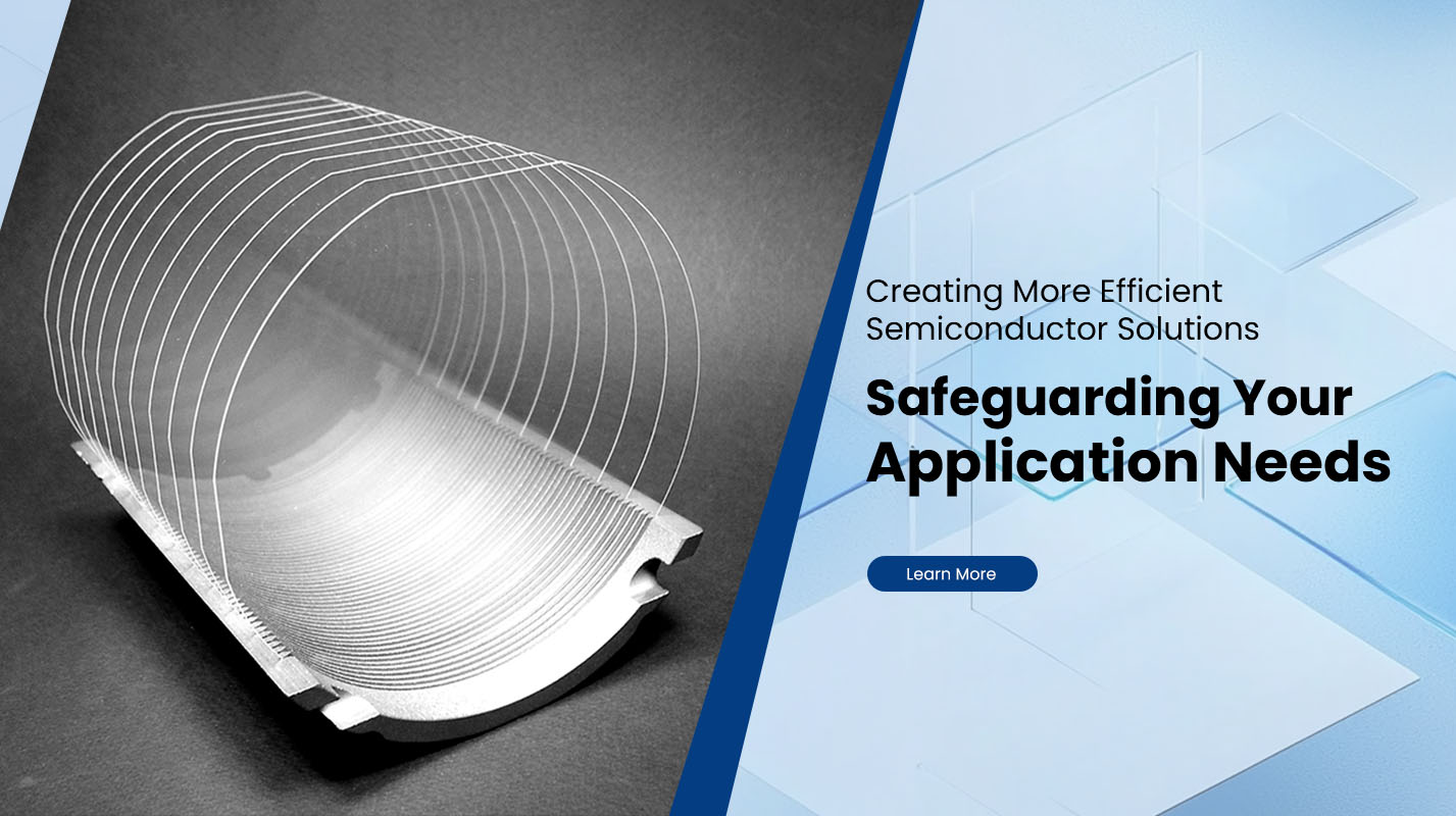
Why Silicon Wafer Is Circular?
Silicon Wafers are essential in the semiconductor industry. They serve as the substrate upon which microelectronic devices—like microprocessors, memory, sensors—are built. One question often asked is: why are silicon wafers circular (round) rather than square or another shape? This article explains the physics, manufacturing process, economic and structural reasons behind the circular shape, with reference to advanced suppliers like Plutosemi.
1. Crystal Growth: The Ingot is Cylindrical
The starting point is a seed crystal which is dipped into molten ultra-pure silicon. Using processes such as the Czochralski growth method, the seed is pulled while rotating, causing the molten silicon to solidify into a single-crystal ingot (also called a boule). Because the seed and/or crucible rotate, the natural geometry formed is cylindrical.
From that cylindrical ingot you cut slices (wafers). You simply slice disks from the cylinder. Thus the wafers are circular by nature of their origin.
2. Uniformity, Mechanical and Thermal Advantages
Circular shape helps in uniform distribution of stress and temperature. Edges of a circle are all at the same distance from the center; there are no sharp corners. Sharp corners tend to concentrate stress, leading to possible cracking or defects. Especially under high temperature, mechanical handling, or during polishing / chemical treatments, round edges are more robust.
During processes like photoresist coating, etching, deposition, spinning etc., wafers are often rotated. A round wafer rotates more smoothly, with more uniform radial distribution of fluid, chemicals, or heat. Corners on a non-circular wafer would complicate fluid flow, may lead to non-uniformity.
3. Manufacturing and Cost Efficiency
Given that the ingot is cylindrical, making round wafers avoids needing to cut away large portions of material just to shape it into a square, which would waste silicon and increase cost.
Tools and equipment across the semiconductor fabrication process—sawing, polishing, chemical-mechanical planarization (CMP), lithography—are designed for round wafers. Switching to other shapes would require redesign of much of the tooling and infrastructure. That’s a large cost, and the benefit (if any) has not outweighted the cost so far.
4. Waste and Yield Considerations
Although round wafers do lead to “edge losses” (some area around the circumference from which full dies cannot be obtained), these losses are outweighed by the advantages of circular shape. Many dies are square or rectangular, so there is “dead” area around the edge; but for round vs square wafer, the trade-off favors round because of the ingot shape, uniformity, mechanical stability, and lower cost.
5. Historical Path-Dependency & Industry Standards
Circular wafers have been standard for decades, ever since methods like Czochralski were developed. Industry bodies set standards (e.g. SEMI standards) for wafer diameters (100 mm, 150 mm, 200 mm, 300 mm, etc.), flat or notch for orientation, etc.
Because fabs, handling, transport, robotics, and process tools are all optimized for these sizes and shapes, changing to a different shape would mean retooling, adaptation, and potential compatibility problems.
6. What About Alternatives?
Square or rectangular wafers could reduce edge waste, pack dies more “tightly” in theory. But the corners are fragile, more prone to chipping and breakage. Handling and thermal expansion stresses are more complicated.
Hexagonal shapes have been considered in concept (for example, better packing efficiency), but again ingots are cylindrical, requires substantial reengineering, and corners still present issues. So far no major shift in industry practice.
7. Plutosemi: Advanced Production & High-Precision Round Wafers / SOI
Here’s how Plutosemi fits into this:
As a company offering high-quality silicon wafers and SOI (Silicon On Insulator) products, Plutosemi leverages advanced production processes to deliver wafers with high precision in thickness, flatness, defect density, and orientation.
Because the industry standard and equipment are designed for circular wafers, Plutosemi’s expertise in producing round wafers and SOI wafers means compatibility with global fabs, supply chain, and downstream users.
Plutosemi is positioned well to offer tailored wafers for diverse applications: from standard CMOS, MEMS, sensors, to advanced devices needing very tight tolerances. Using circle-based wafer production allows for optimized yield, fewer mechanical issues, and better handling. For details, you can browse Plutosemi’s product offerings at https://www.plutosemitech.com.
8. Summary
In summary, silicon wafers are circular because:
Crystal growth produces cylindrical ingots, making disks natural.
Circular wafers distribute stress & temperature more evenly; they avoid weak corners.
Manufacturing, handling and coating (spinning etc.) are more uniform with circle shapes.
Cost efficiency and material-waste trade-offs favor circular over other shapes.
Industry standards and infrastructure are built around round wafers.
While “edge waste” exists, the overall benefits make the round wafer shape optimal given current technologies and supply chains.


