How Long Does It Take to Make a Silicon Wafer?
Silicon Wafers are the foundation of nearly every semiconductor device—from microprocessors to solar cells. Yet many people don’t realize how long and complex the wafer production process is. In this article, we break down the steps, timing, and factors affecting how long it takes to go from raw silicon to a finished wafer. We also touch on how companies like Plutosemi are involved in this advanced manufacturing chain.
What Is A Silicon Wafer?
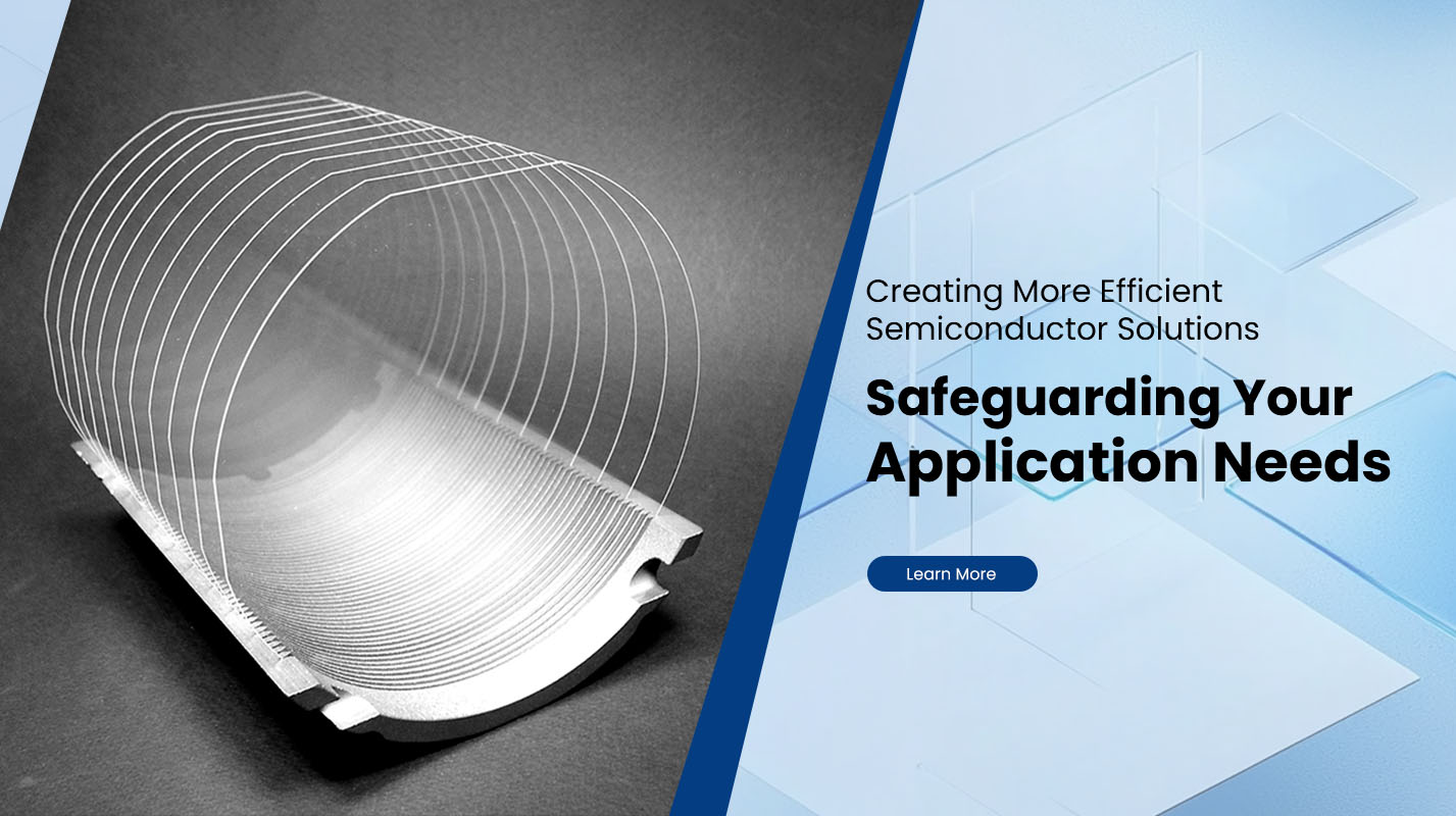
A silicon wafer is a thin slice of semiconductor-grade crystalline silicon, used as the substrate for fabricating microelectronic devices. To meet the high purity, crystalline perfection, flatness, and thickness uniformity needed, wafers undergo many steps—each precise and often time‐consuming.
Main Steps in silicon wafer manufacturing
Here are the core stages, and roughly how long each usually takes:
| Stage | Description | Approximate Time* |
|---|---|---|
| Silicon Purification & Poly-Si Production | Raw silicon is refined to semiconductor purity (99.9999%+), then made into polycrystalline silicon blocks. | Weeks to months |
| Crystal Growth (Ingot / Boule Growth) | Using methods like the Czochralski (CZ) or Float Zone (FZ) process, a single‐crystal ingot or boule is grown. Requires precise temperature, seed crystal alignment, uniform doping, etc. | ~ 1 week up to a month depending on diameter, quality, and growth method. |
| Cooling and Annealing | Once growth is complete, the crystal needs to cool slowly to avoid defects and dislocations. May include thermal treatments. | Several days |
| Slicing / Wafering | The ingot is sliced into wafer slices using wire saws or other tools, usually about 0.5–1 mm thick, then cleaned. | 1–2 days |
| Lapping, Grinding, and Polishing | Wafer surfaces are ground and polished to achieve flatness and smoothness; edges are rounded; thickness uniformity is achieved. | 1–2 days |
| Cleaning & Surface Preparation | Cleaning to remove particles, organic/inorganic contamination; sometimes oxide formation or removal; sometimes deposition of passivation layers. | Hours to a day |
| Inspections and Quality Control | Visual, optical, and sometimes microscopic or electron‐microscopic inspection for defects, warpage, flatness, etc. | Hours to a day |
* These times are approximate and can vary significantly based on wafer size, wafer type (e.g. standard vs. ultra‐thin), diameter (150 mm, 200 mm, 300 mm, etc.), and quality class (standard, prime, electronic grade, etc.).
From Wafer to Finished Chips: Fabrication Cycle Time
It’s important to distinguish making the wafer substrate from fabricating devices on the wafer (the “fab” process). Once you have a polished, clean wafer, the steps to build semiconductor devices (photolithography, doping, deposition, etching, metallization, etc.) take much longer.
For modern, advanced semiconductor manufacturing, the wafer fabrication process (device build, not just substrate) typically takes 11-13 weeks on average, sometimes up to 15 weeks for more advanced nodes.
The overall “cycle time” from blank wafer + device processing to finished wafer(s) may be about 12 weeks, sometimes longer (14-20 weeks) depending on the complexity, yield, and technology node.
So, How Long to Make Just the Wafer Itself?
If you isolate only the substrate wafer production (not the device fabrication on top), a rough estimate:
For a standard 300 mm single-crystal wafer: approximately 2–6 weeks from raw silicon/purification to a clean, polished, inspected wafer ready for device processing.
If higher specifications (thicker, larger diameter, ultra‐low defect densities, special doping or crystal orientation) come into play, it can stretch toward the longer end of that range or beyond.
Factors That Can Speed Up or Slow Down Wafer Production
Some of the variables that affect timing:
Wafer diameter and thickness: Larger diameter (e.g. 300 mm vs. 150 mm) takes longer growth, handling, and yields are more challenging.
Crystal growth method: CZ vs FZ have different rates, costs, and defect profiles.
Purity and defect tolerances: More stringent specs require more careful growth, slower rates, extra inspections.
Yield & rejection rates: Wafers with defects may be discarded or reworked, which increases effective time if yield is low.
Equipment throughput & cleanroom capacity: Bottlenecks in slicing, polishing, or cleaning steps can delay the pipeline.
Supply chain and material quality: If raw materials (e.g. high-purity silicon, dopants, crucibles) or tools are delayed, that adds lag.
Why It Matters: Impacts for the Semiconductor Industry & Customers
Cost: Time = cost. Longer wafer production raises material, labor, utility, and equipment costs.
Lead time and supply chain: Companies buying wafers or devices need to plan many weeks ahead.
Technological innovations: Faster growth, better polishing, automation in handling, etc., can reduce times.
Quality trade-offs: Speed must sometimes be sacrificed for higher yield, fewer defects.
Plutosemi’s Role & Capabilities
At Plutosemi, we operate in this challenging semiconductor supply chain. Our company is committed to:
Sourcing ultra-high purity raw silicon and managing supply to avoid delays.
Working with advances in crystal growth, wafer surface conditioning, and polishing to deliver wafers meeting tight specifications.
Maintaining high yield and low defects so that our customers benefit from faster turnaround and reliability in their downstream device fabrication.
Because of the number of steps involved and the precision required, we at Plutosemi aim to optimize each stage—from ingot growth to wafer polishing—to reduce time without sacrificing quality.
Summary
Making the substrate wafer itself typically takes 2-6 weeks, depending on size, quality, and complexity.
Device fabrication on that wafer adds many more steps; full wafer + device cycle time is often 11-15 weeks or more for advanced nodes.
Many factors influence this: wafer diameter, defect tolerance, throughput, yield, equipment capacity, and material supply.
Previous: What Does a Silicon Wafer Look Like?


