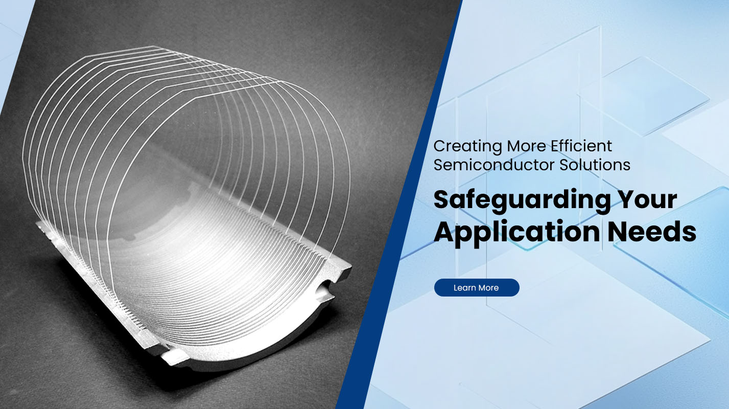
What Does a Silicon Wafer Look Like?
When people think about the foundation of modern electronics, the Silicon Wafer often comes to mind. This thin slice of highly purified silicon acts as the base material for semiconductors, which power everything from smartphones and computers to solar panels and advanced automotive systems. But what exactly does a silicon wafer look like, and how can you recognize one? Let’s break it down.
Appearance of a Silicon Wafer
A silicon wafer is typically circular and ultra-thin, resembling a mirror-like disk. The most common diameters range from 100mm (4 inches) to 300mm (12 inches), although research applications may use smaller wafers and advanced fabs are pushing toward 450mm wafers. The surface is polished to a near-perfect smoothness, creating a highly reflective and shiny finish that can appear metallic at first glance.
The color of a silicon wafer can vary depending on the thickness and the way light reflects on its surface. Under certain lighting conditions, it may look silvery, dark gray, or even iridescent, with rainbow-like patterns due to light interference across the wafer’s extremely flat surface.
Structural Features
Flat or Notched Edge: Most silicon wafers feature a flat edge or a small notch on the rim. This is not for decoration but to indicate crystal orientation and doping type. For example, a flat edge helps manufacturers quickly identify how the silicon lattice is aligned.
Mirror Finish: Prime-grade wafers are polished to a level where imperfections are measured in nanometers. This reflective surface is critical for successful photolithography during semiconductor manufacturing.
Thickness: Despite their large diameter, silicon wafers are surprisingly thin. A 300mm wafer is usually less than 1mm thick, making it lightweight yet fragile.
How Silicon Wafers Are Made
To understand why they look the way they do, it’s important to note the manufacturing process. Silicon wafers are sliced from a cylindrical silicon ingot grown using methods like the Czochralski process. After slicing, they are ground, etched, and polished to achieve perfect flatness and cleanliness. This is why the finished wafer appears so smooth and reflective.
Visual Variations in Silicon Wafers
Bare Silicon Wafer
Appears silver-gray, metallic, and glossy.
No patterns are visible until processing begins.
Processed Silicon Wafer
After layers of oxide, metal, and photoresist are added, the wafer may show intricate grid-like circuit patterns.
These patterns can appear colorful due to thin-film interference effects.
Test or Dummy Wafer
Often less polished and may appear matte rather than mirror-like.
Used in equipment calibration rather than active device production.
Why Silicon Wafer Appearance Matters
The visual characteristics of a silicon wafer are more than just aesthetics. The smooth, reflective surface ensures accurate photolithography alignment, while the notch or flat edge guarantees consistent orientation during high-volume semiconductor production. Even slight surface defects, scratches, or contamination visible under magnification can render a wafer unusable.
Applications Where You’ll See Silicon Wafers
Semiconductor Fabs: Large polished wafers stacked in carriers before being processed into integrated circuits.
Solar Industry: Thinner crystalline silicon wafers cut into smaller cells used for photovoltaic panels.
Research Labs: Small-diameter wafers for prototyping MEMS (Micro-Electro-Mechanical Systems), sensors, and optics.
Conclusion
So, What Does a Silicon Wafer Look Like? Imagine a perfectly round, thin, mirror-like disk with either a notch or flat edge for orientation. Its metallic-gray or iridescent surface is a result of extreme polishing and precision engineering. Though fragile and unassuming at first glance, this disk is the cornerstone of the modern digital world.
If you’re looking to source high-quality silicon wafers for semiconductor manufacturing, research, or solar applications, understanding their appearance is the first step toward identifying the right type for your needs.


