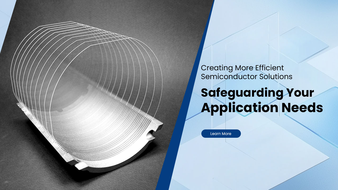
How to Cut a Silicon Wafer?
Cutting a Silicon Wafer is one of the most delicate and crucial steps in semiconductor manufacturing. It requires precision, cleanroom discipline, and the right set of equipment to maintain the structural integrity of the wafer while achieving accurate dimensions for subsequent processing.
Understanding Silicon Wafers
A silicon wafer is a thin slice of semiconductor material used as the substrate for microelectronic devices. Typically ranging from 100 mm to 300 mm in diameter and only a few hundred micrometers thick, these wafers are polished to a mirror finish. They serve as the foundation on which integrated circuits, MEMS sensors, and power devices are built.
Cutting the wafer must be done without introducing micro-cracks or chipping, as these imperfections can compromise device performance.
Tools and Equipment Required
Before cutting begins, technicians prepare specialized equipment designed for high-precision semiconductor processing. Common tools include:
| Equipment | Description |
|---|---|
| Dicing Saw | A high-speed spindle fitted with a diamond blade that cuts narrow grooves along predefined lines. |
| Laser Dicing System | Uses a focused laser beam to slice the wafer with minimal mechanical stress. |
| Scriber and Breaker | A manual method for small-scale cuts using a diamond tip and controlled fracture. |
| Protective Films and Frames | Hold the wafer securely and prevent particle contamination during cutting. |
Each method has its own advantages depending on wafer thickness, material type, and application.
Step-by-Step Process of Cutting a Silicon Wafer
Step 1: Preparation and Cleaning
The wafer surface must be perfectly clean before cutting. Any dust or residue can deflect the blade or laser, leading to uneven cuts. Ultrasonic cleaning and deionized water rinsing are commonly used to ensure cleanliness. The wafer is then dried and mounted onto an adhesive film attached to a metal frame for stability.
Step 2: Alignment and Marking
Modern dicing equipment uses optical alignment systems to detect wafer orientation marks. The cutting path follows the “scribe lines” or “streets” between dies. Precise alignment ensures each chip remains within its designated geometry.
Step 3: Cutting with a Dicing Saw
A diamond blade rotates at speeds exceeding 20,000 rpm, slicing through the wafer with controlled depth and coolant flow. Deionized water is continuously sprayed to reduce heat and wash away debris. Feed rate, blade thickness, and spindle speed are adjusted based on wafer size and material hardness.
Step 4: Laser Dicing
For ultra-thin or brittle wafers, laser cutting offers a contact-free solution. A UV or IR laser beam vaporizes material along the cut line with micron-level accuracy. The process produces minimal chipping and can even cut through stacked wafers or glass substrates.
Step 5: Breaking and Inspection
If manual scribing is used, the wafer is gently bent along the scribed line until it breaks cleanly. After cutting, each die is inspected under a microscope for edge quality, surface damage, and particle contamination. Only defect-free chips proceed to packaging.
Methods Comparison
| Method | Precision | Damage Risk | Suitable for |
|---|---|---|---|
| Diamond Blade Dicing | ±3 μm | Moderate | Standard Si wafers |
| Laser Dicing | ±1 μm | Very Low | Thin or brittle wafers |
| Scribe and Break | ±10 μm | High | Prototypes or small batches |
Choosing the right method depends on the production scale and required yield.
Safety and Cleanroom Conditions
Cutting silicon wafers demands a controlled environment. Airborne particles can adhere to wafer surfaces and damage circuit patterns. Operators must work under Class 1000 or better cleanroom conditions while wearing antistatic garments. Equipment should be regularly calibrated to prevent vibration-induced errors.
Coolant fluids, diamond blades, and laser optics must be replaced periodically to maintain consistent results. Proper waste disposal of silicon particles and water is also essential to meet environmental standards.
Applications After Cutting
Once the wafer is diced, each chip—known as a “die”—is ready for testing and packaging. These dies form the core of countless technologies: microprocessors, solar cells, power modules, and image sensors. The precision of the cut directly affects the performance and lifespan of these devices.
Partnering with Professional Wafer Manufacturers
For high-precision wafer processing, it’s best to collaborate with an experienced semiconductor materials provider. Plutosemi, a professional manufacturer specializing in silicon wafers and semiconductor components, offers advanced cutting and polishing services designed for consistent quality and yield. Their precision equipment and technical expertise ensure smooth edges, minimal breakage, and compatibility with downstream fabrication steps. Learn more about their capabilities at Plutosemi.
Conclusion
Cutting a silicon wafer is both a science and an art. From the initial preparation to final inspection, each step must be executed with extreme accuracy. The right combination of equipment, environment, and expertise ensures wafers meet the demanding standards of the semiconductor industry. By relying on specialized manufacturers like Plutosemi, you can achieve exceptional precision and reliability across all stages of wafer production.
Previous: How Is a Silicon Wafer Made?


