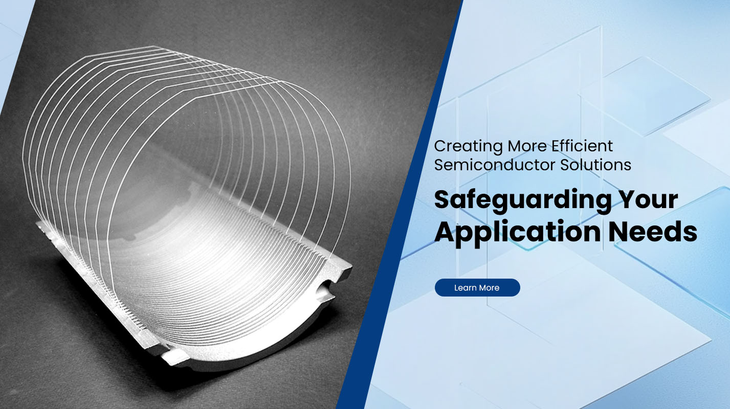
What Applications Use Sapphire Wafers?
Sapphire Wafers, made from single-crystal aluminum oxide (Al₂O₃), combine unique optical, electrical, thermal, and mechanical properties. Because of these advantages, they are widely adopted across many high-tech fields. Below is a survey of their major uses, technical benefits, and emerging trends.
Key Properties That Enable Wide Use
Before exploring applications, here are the critical features that make sapphire wafers attractive:
Optical transparency from deep ultraviolet to infrared (roughly 0.2 µm to 5 µm or more)
Exceptional hardness and scratch resistance (Mohs hardness ~9)
Thermal stability (melting point ~2,030 °C) and good thermal conductivity
Excellent electrical insulation and chemical inertness
Low defect density and crystallographic uniformity when properly grown and processed
Because of this combination of traits, sapphire wafers are used in harsh environments, in optical systems, and in advanced semiconductor structures.
Major Application Areas
1. LED and Optoelectronic Devices
One of the most widespread uses of sapphire wafers is as a substrate for GaN-based LEDs. The lattice match, thermal stability, and manufacturability make sapphire a default choice in LED production.
To enhance light extraction, many LED manufacturers use patterned sapphire substrates (PSS), which incorporate microstructured patterns on the sapphire surface to reduce defects, scatter light favorably, and boost internal quantum efficiency and extraction efficiency.
Variants like c-plane patterned sapphire, r-plane, and m-plane are used depending on the desired polarity and emission performance.
2. Semiconductor Devices & Insulating Substrates
Sapphire wafers serve as insulating substrates in devices where electrical isolation is critical — for instance, in radio-frequency devices, high-power electronics, and hybrid structures.
A notable technology is silicon-on-sapphire (SOS), where a thin layer of silicon is grown or bonded onto a sapphire wafer. This allows for CMOS circuits with excellent isolation, lower parasitic capacitance, and radiation hardness, making it suitable for high-reliability or aerospace applications.
In advanced quantum and superconducting circuits, sapphire is also being explored as a low-loss dielectric substrate, supporting devices such as Josephson junctions, superconducting qubits, and high-coherence circuits.
3. Optical Windows, Lenses, and Cover Glass
Because of its optical clarity across a broad spectral band, sapphire is used in windows, lenses, and protective covers in optical systems, sensors, and imaging devices.
Examples include:
Transparent protective windows in harsh environments (e.g., high temperature, plasma, vacuum)
Camera and sensor cover glass or lens elements for wearables, smartphones, or industrial sensors, where scratch resistance and durability matter
Optical components such as prisms, waveplates, and windows for spectrometers across UV to IR bands
4. Harsh-Environment Windows & Observation Ports
In systems with high temperature, high pressure, or aggressive chemistry (e.g., plasma reactors, furnaces, etchers), sapphire is used as viewports and chamber windows thanks to its resilience.
It also appears in aerospace and defense systems as transparent armor or in radome windows, combining light transmissivity with mechanical strength.
5. Medical, Scientific & Measurement Devices
In medical devices, sapphire is used for endoscope lens covers, laser delivery rods, filters, and even implantable components, owing to its biocompatibility, purity, and stability.
Scientific instrumentation also benefits: sapphire windows are used in spectroscopy over UV to IR, and laboratory equipment employs sapphire components to survive harsh chemical environments.
6. Mechanical Components, Supports & Handling Parts
Because sapphire is chemically inert, thermally stable, and dimensionally stable, it is used for structural or support parts in semiconductor fabrication, such as lift pins, wafer carriers, chambers, rods, and shelf plates.
In particular, sapphire shelves (firing setters) are used in high-temperature furnaces to reduce contamination and warpage compared to ceramic alternatives. Sapphire tubes and containers also allow visual monitoring in corrosive or high-temperature processes.
Comparative Table: Application vs. Key Enabling Sapphire Property
| Application Domain | Main Sapphire Advantage | Typical Use Cases |
|---|---|---|
| LEDs / optoelectronics | Lattice match, transparency, thermal management | GaN growth, patterned substrates |
| Electronic devices (insulating) | Electrical isolation, thermal stability | SOS, RF circuits, superconducting devices |
| Optical components | Broad-band transparency, scratch resistance | Windows, lenses, prisms, sensor covers |
| Harsh-environment windows | High temperature & chemical resistance | Chamber windows, radomes, viewport systems |
| Medical / science | Biocompatibility, purity, durability | Endoscopes, filters, laser optics |
| Structural/handling parts | Mechanical strength, inertness | Lift pins, shelves, carriers, tubes |
Emerging Trends & Research Frontiers
Quantum and superconducting circuits: Sapphire’s ultra-low dielectric loss makes it well suited for high-coherence qubits and scalable quantum hardware. Techniques for machining through-substrate vias (TSVs) in sapphire are under development to enable signal routing in thick sapphire wafers.
Graphene and two-dimensional materials: Direct growth of large-area graphene on sapphire wafers has been demonstrated, showing potential for integrating 2D materials without metal catalysts.
Higher diameter wafers & improved patterns: As display, LED, and photonics industries push for larger and more complex substrates, sapphire wafer manufacturers are scaling production, refining patterning techniques, and improving surface quality.
Integration in harsh environments and aerospace: Sapphire windows and transparent armor continue to see adoption in systems requiring durability, multi-spectral transparency, and mechanical protection.
Why Choose a Reliable Supplier?
Because sapphire wafers must meet extremely tight specifications (surface roughness, flatness, crystallographic orientation, contamination levels), choosing a trusted supplier is vital. A high-quality provider will offer custom sizes, off-cut angles, cleanroom packaging, and partner with you on device integration.
If your design or manufacturing process requires specialty wafers, consider Plutosemi (from Plutosemitech). They offer semiconductor-grade substrates, precision processing, and customization to support advanced applications in electronics, photonics, and beyond. Plutosemi provides more info about their product offerings and capabilities.
Conclusion
Sapphire wafers occupy a unique niche in high-end electronics and optics. Their blend of optical clarity, thermal and mechanical robustness, electrical insulation, and chemical inertness makes them indispensable across LEDs, optoelectronics, harsh-environment windows, precision optics, and emerging quantum systems. When paired with the right suppliers—like Plutosemi—they open possibilities for innovation in demanding technological applications.


