How Are Wafers Tested Before Packaging?
In semiconductor manufacturing, wafer testing is a crucial step that ensures only functional and high-quality chips proceed to the packaging stage. This process, often referred to as wafer probing or wafer sort, identifies defective dies early, minimizing material waste and improving production efficiency. Each wafer undergoes a series of electrical and physical evaluations to verify that the integrated circuits perform as designed before being separated into individual chips.
Wafer Testing Overview
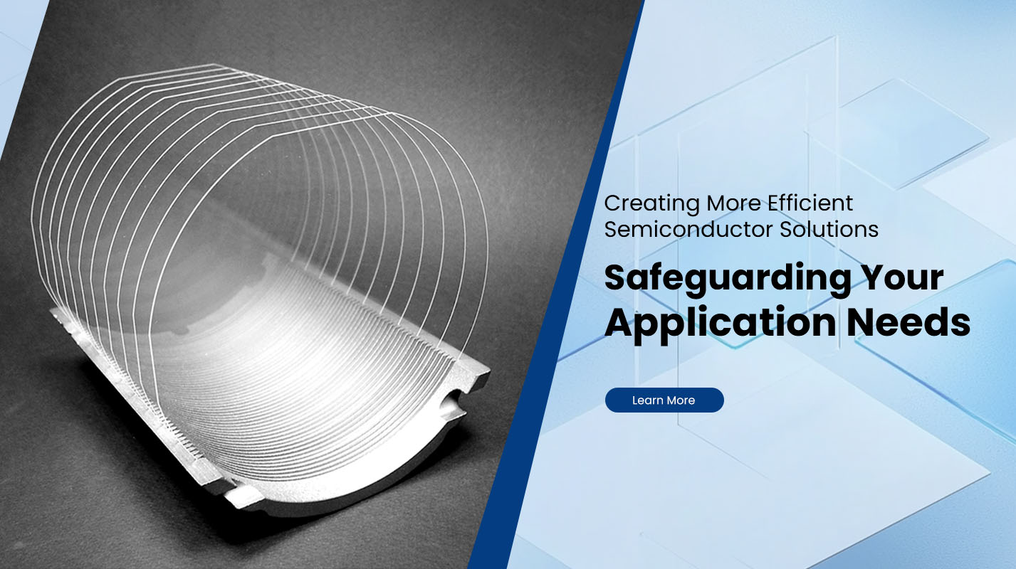
Before packaging, a Silicon Wafer—containing hundreds or even thousands of tiny integrated circuits—is carefully examined using automated test equipment (ATE). These machines connect to the wafer through a probe card, which makes direct contact with the contact pads of each die. Through this contact, voltage and signal measurements are performed to detect functional or parametric defects.
The goal is to classify every die into different categories such as “good,” “marginal,” or “defective.” This data is recorded in a wafer map, which later guides the dicing and assembly processes. The result is a more efficient manufacturing workflow where only verified good dies move forward for packaging and final testing.
Key Steps in Wafer Testing
Visual Inspection
Before electrical testing, wafers undergo microscopic inspection to check for visible defects such as surface scratches, particle contamination, or lithographic misalignments. Automated optical inspection (AOI) systems are used to identify these defects quickly and accurately.
| Inspection Type | Purpose | Equipment Used |
|---|---|---|
| Surface scan | Detect micro-cracks and contamination | AOI, SEM |
| Pattern inspection | Check alignment and layer consistency | Optical microscopes |
| Defect classification | Identify causes and defect density | Image analysis software |
Electrical Wafer Sort
Electrical testing measures the electrical performance of each die using parameters such as leakage current, threshold voltage, and functional response to input signals. This stage verifies that transistors, resistors, and capacitors on the wafer meet design specifications.
Automated testers simulate operating conditions to ensure that chips will perform reliably once packaged. Failing dies are marked on the wafer map to prevent them from being assembled later.
Parametric Testing
Parametric testing evaluates specific device parameters at the wafer level, including resistance, capacitance, and current-voltage characteristics. These measurements provide valuable feedback for process engineers to monitor production quality and adjust fabrication conditions if necessary.
For instance, variations in transistor threshold voltage or leakage current may indicate a process drift that needs correction before subsequent batches are produced.
Functional Testing
Functional testing verifies the actual operation of each integrated circuit according to its intended logic or analog behavior. It ensures that all components on the chip interact properly and that the design performs as expected under test conditions. This testing phase may also simulate temperature and power variations to detect reliability issues early.
Wafer Mapping and Data Analysis
After testing, all results are compiled into a digital wafer map. Each die’s status is color-coded—typically green for good, red for bad, and yellow for marginal. The wafer map becomes an essential reference for downstream processes like die cutting, packaging, and final test. Advanced analytics systems use this data to predict yield, trace root causes, and continuously optimize the fabrication process.
Benefits of Early Wafer Testing
Wafer-level testing provides significant benefits to semiconductor manufacturers:
Yield Optimization: Early identification of defects helps prevent wasteful packaging of non-functional chips.
Cost Efficiency: Testing at the wafer level saves time and materials by isolating issues before assembly.
Process Control: Data gathered from wafer tests enables process engineers to fine-tune manufacturing parameters.
Reliability Assurance: Only fully verified dies continue to packaging, ensuring high performance and long-term reliability for end users.
Modern Wafer Testing Technologies
The semiconductor industry continues to innovate wafer testing techniques. Probe cards now feature micro-needles and MEMS structures for better contact accuracy, while ATE systems can handle advanced nodes below 5 nm. In addition, artificial intelligence is increasingly used for defect classification and predictive yield analysis.
Advanced test solutions also integrate temperature control and multi-site testing, allowing several dies to be tested simultaneously. This accelerates throughput and lowers per-unit cost without compromising accuracy.
Conclusion
Wafer testing before packaging plays a decisive role in semiconductor quality assurance. Through visual inspection, electrical probing, and detailed parametric analysis, manufacturers ensure that only the best chips reach customers. It serves as the bridge between fabrication and packaging, preserving both performance and cost efficiency across the production chain.
For businesses seeking reliable wafer testing and semiconductor solutions, Plutosemi provides advanced process control systems and precision testing services tailored for high-performance wafer manufacturing. Their expertise helps clients achieve consistent yield improvement and superior chip reliability from start to finish.


