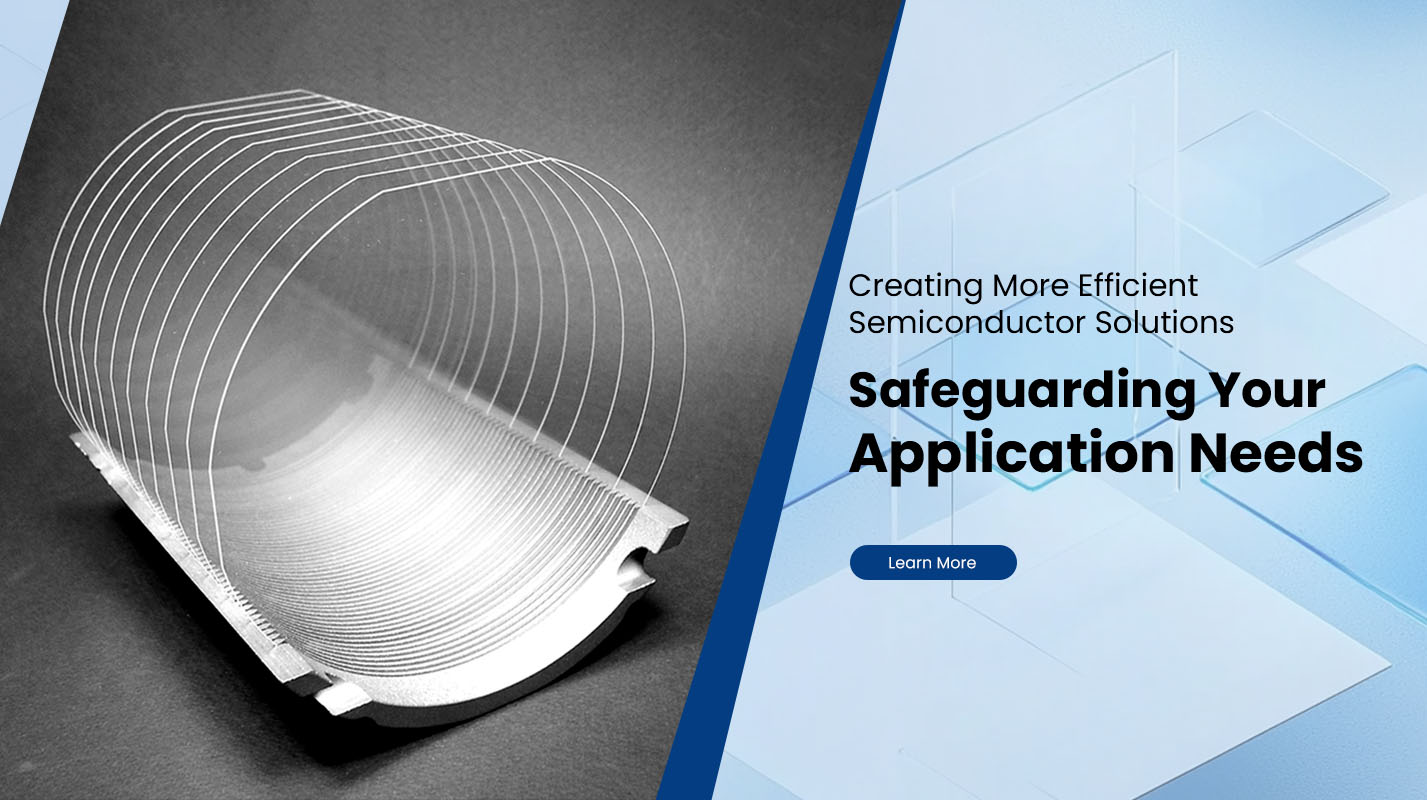
What Are the Packaging Options for Silicon Wafers?
Silicon Wafers are among the most delicate and valuable components in the semiconductor industry. Their packaging plays a vital role in ensuring safe transportation, preventing contamination, and maintaining structural integrity throughout the production chain. As technology nodes become smaller and wafer diameters increase, packaging solutions have evolved from simple trays to highly engineered protective systems that meet stringent cleanroom standards.
Importance of Proper Silicon Wafer Packaging
The wafer surface is extremely sensitive to particles, scratches, and static discharge. Improper packaging can lead to surface damage, contamination, or stress fractures that compromise yield rates. Hence, choosing the right packaging is not just a logistics decision but a critical quality control step. Proper packaging allows wafers to be safely shipped across long distances and stored under cleanroom conditions without performance degradation.
Common Packaging Types
Several packaging options are used depending on wafer size, application, and transport requirements. Below are the most common solutions in today’s semiconductor supply chain.
1. Wafer Shipping Boxes
Wafer shipping boxes, often made of high-purity polypropylene (PP) or polycarbonate (PC), are the standard solution for handling 6-inch, 8-inch, and 12-inch wafers. These boxes feature an inner cassette or ring frame that holds wafers securely in slots. They are designed to withstand vibration and mechanical shock while maintaining ISO Class 5–7 cleanliness. Most are vacuum-sealed in antistatic polyethylene bags before shipment.
2. Front Opening Shipping Boxes (FOSB)
FOSB containers are primarily used for 300 mm wafers and are compatible with automated wafer handling systems. They feature front doors with sealing gaskets and purge valves to maintain clean, dry nitrogen environments. A FOSB can hold up to 25 wafers in precisely aligned slots. The design prevents direct handling of wafers and minimizes the risk of particle generation during loading and unloading.
3. Wafer Carriers and Cassettes
For smaller wafer diameters (100 mm to 200 mm), open wafer carriers or cassettes made of static-dissipative materials are common. They are used within fab environments for short-distance transfer between process stations. Wafer carriers are lightweight, reusable, and designed to meet SEMI E47.1 and E62 standards. Their ribs and slots distribute mechanical stress evenly to avoid micro-cracking.
4. Vacuum-Sealed Bags
Vacuum packaging is often combined with rigid boxes to create a secondary protection layer. Wafers are first placed in carriers, which are then sealed inside multilayer antistatic vacuum bags with desiccants. This configuration eliminates moisture ingress and airborne particles, ensuring that surface oxidation and ionic contamination are minimized during long-distance transportation or extended storage.
5. Single Wafer Pouches
For high-value or prototype wafers, single-wafer pouches are used. These are made of soft, non-abrasive cleanroom films with ESD protection. They protect against scratches and mechanical contact, ideal for R&D or low-volume shipments. Each pouch is usually sealed and labeled with wafer ID, thickness, and flat orientation, making traceability straightforward in cleanroom logistics.
6. Customized Multi-Layer Crates
When wafers need to be shipped in bulk or under extreme environmental conditions, customized crates are used. These include multiple layers of vibration-absorbing foam, moisture barriers, and internal stacking systems. Such crates are often designed according to customer specifications and tested under simulated transport conditions to ensure mechanical safety.
| Packaging Type | Typical Capacity | Material | Protection Level |
|---|---|---|---|
| Wafer Shipping Box | 25 wafers | PP / PC | High |
| FOSB | 25 wafers | Polycarbonate / PFA | Very High |
| Wafer Cassette | 25 wafers | ESD Plastic | Medium |
| Vacuum Bag | 1–25 wafers | Antistatic Film | High |
| Single Wafer Pouch | 1 wafer | Soft Film | Very High |
| Multi-Layer Crate | 25–100 wafers | Mixed Materials | Maximum |
Key Performance Factors
When selecting a wafer packaging method, several technical factors must be evaluated:
Cleanliness: All materials should meet Class 100 or better standards to prevent particle contamination.
Static Dissipation: Surfaces must maintain surface resistivity between 10⁶–10⁹ Ω to prevent electrostatic discharge damage.
Mechanical Strength: The package must withstand acceleration forces above 10 g during transportation.
Moisture Control: Desiccant and nitrogen purge options help maintain humidity below 5 % RH.
Traceability: Barcode and RFID labeling are essential for automated wafer tracking systems.
Environmental and Reusable Packaging Options
To reduce costs and environmental impact, many fabs are adopting reusable wafer packaging. Reusable boxes and cassettes can undergo ultrasonic cleaning and inspection cycles before being redeployed. Advanced polymers with low outgassing and chemical resistance allow multiple cleaning cycles without deformation. This approach not only cuts material waste but also ensures stable cleanliness levels for repeated usage.
Custom Packaging for Special Applications
Some wafers require customized packaging due to non-standard sizes or sensitive coatings. Manufacturers may offer specialized designs such as:
Vacuum-sealed aluminum foil pouches for ultra-thin wafers
Gel-film carriers for fragile MEMS or sensor wafers
Temperature-controlled crates for long-distance air transport
Such solutions are tailored through 3D modeling and stress analysis to ensure perfect fit and mechanical safety during shipment.
Future Trends in Wafer Packaging
As wafer diameters move toward 450 mm and 3D integration becomes more complex, next-generation wafer packaging will integrate smart sensors for temperature, humidity, and shock monitoring. Intelligent packaging systems will enable real-time tracking of wafer conditions from cleanroom to customer site, improving transparency and yield predictability.
Conclusion
The choice of packaging for silicon wafers directly affects their quality and production yield. From basic polypropylene boxes to advanced FOSB and vacuum-sealed systems, each solution is designed to maintain wafer purity and mechanical stability throughout logistics and storage. For fabs and semiconductor distributors seeking reliable and customizable wafer packaging solutions, Plutosemi provides precision-engineered packaging options and cleanroom handling systems that comply with international SEMI standards.


