How to Choose the Right Glass Wafer?
In the semiconductor and micro-electromechanical systems (MEMS) industries, Glass Wafers play a crucial role in precision manufacturing. They provide electrical insulation, chemical resistance, and optical transparency required for modern sensors, microchips, and optoelectronic devices. Selecting the right glass wafer ensures stable device performance and long-term reliability. Understanding the key parameters and application demands helps engineers and buyers make informed decisions.
Understanding Glass Wafer Basics
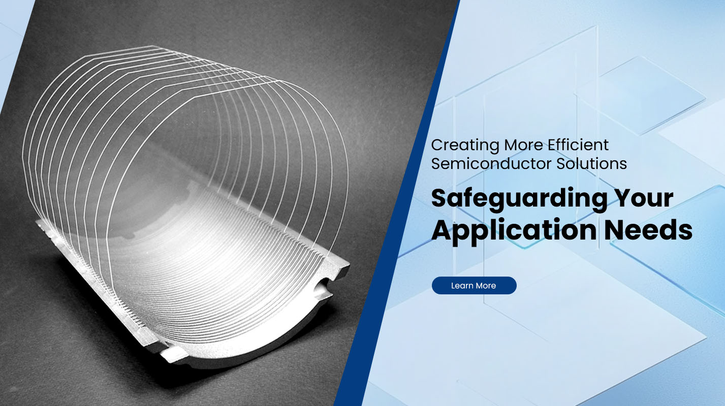
A glass wafer is a thin, precisely polished disk made from specialty glass materials such as borosilicate, fused silica, or aluminosilicate. It typically ranges from 100 mm to 300 mm in diameter and 0.3 mm to 1 mm in thickness. These wafers serve as substrates or bonding partners for Silicon Wafers in MEMS fabrication, optical filters, and sensor packaging. The glass type, purity, and surface finish directly affect dimensional stability and optical clarity, which in turn determine the device’s yield and functionality.
Material Selection and Properties
Choosing the proper glass composition is the first step. Each type has distinct advantages depending on the operating environment and design goals.
| Glass Type | Coefficient of Thermal Expansion (CTE) | Transmission Range | Main Advantages |
|---|---|---|---|
| Borosilicate (e.g., Pyrex) | 3.3 × 10⁻⁶ /K | 300–2500 nm | Excellent thermal stability, low alkali content |
| Fused Silica | 0.5 × 10⁻⁶ /K | 180–3500 nm | Ultra-low CTE, superior UV transparency |
| Aluminosilicate | 5 × 10⁻⁶ /K | 350–2500 nm | High mechanical strength, impact resistance |
| Soda-lime | 9 × 10⁻⁶ /K | 350–2000 nm | Cost-effective for non-critical optical use |
For applications involving direct wafer bonding or thermal cycling, materials with a closely matched CTE to silicon (2.6 × 10⁻⁶ /K) such as borosilicate or fused silica are preferred. When optical transmission in UV or IR ranges is required, fused silica becomes the best choice.
Surface Quality and Flatness
Surface precision determines the wafer’s bonding quality and device alignment. Typical semiconductor-grade glass wafers feature total thickness variation (TTV) below 5 µm and surface roughness (Ra) under 1 nm. For optical or micro-fluidic systems, flatness below 2 µm is often necessary to avoid light scattering and ensure accurate etching. A high-quality polish eliminates micro-scratches that could propagate cracks during subsequent high-temperature processes.
Thickness and Diameter Considerations
The wafer’s size must match the intended fabrication line and mechanical handling system. Standard diameters include 100 mm, 150 mm, 200 mm, and 300 mm. Thinner wafers improve heat transfer and reduce stress but may compromise mechanical strength. Therefore, balancing flexibility with rigidity is critical. For MEMS devices and sensors requiring through-holes or cavities, thicker glass wafers offer better support during etching and dicing.
Optical and Electrical Characteristics
Glass wafers often act as optical windows or insulating layers. Optical transmission from UV to near-IR wavelengths should be verified for the device’s operational spectrum. Similarly, dielectric strength (usually above 10 MV/m) and volume resistivity (>10¹² Ω·cm) ensure safe electrical insulation between conductive layers. Anti-reflection coatings or index-matched bonding layers can further optimize optical performance.
Chemical Resistance and Environmental Stability
Glass wafers are exposed to etchants, cleaning agents, and thermal cycles. High-purity fused silica and aluminosilicate glasses exhibit excellent chemical durability against HF, HCl, and alkalis. In cleanroom environments, resistance to moisture absorption prevents warping and contamination. Long-term stability under varying humidity and temperature conditions is essential for optical alignment and device packaging integrity.
Bonding Compatibility and Fabrication Requirements
Different bonding methods such as anodic bonding, fusion bonding, or adhesive bonding require specific surface properties and thermal limits. For instance, anodic bonding with silicon demands a glass containing sodium ions to facilitate electrostatic joining. Conversely, fusion bonding requires ultra-smooth, particle-free surfaces to achieve atomic-level contact. Understanding process compatibility helps prevent yield loss during mass production.
Mechanical Strength and Edge Profile
Edge quality impacts handling safety and breakage rate. Wafers with chamfered or rounded edges reduce the risk of chipping during automated transport. Mechanical strength is measured by modulus of rupture and fracture toughness; high-end aluminosilicate glass can exceed 600 MPa in bending strength. Strengthened glass through ion-exchange or thermal tempering is recommended for demanding MEMS packaging or display panel applications.
Quality Certification and Traceability
Reliable suppliers provide wafers with complete documentation, including material batch, polishing records, and inspection reports. Certifications such as ISO 9001 and RoHS compliance guarantee consistent production standards. Optical inspection systems and surface interferometers confirm defect-free surfaces and dimensional precision. Full traceability from raw material to shipment ensures long-term supply stability for OEM partners.
Partnering with a Trusted Manufacturer
Selecting a dependable manufacturing partner is just as vital as the wafer specifications themselves. A qualified supplier should offer customized wafer thicknesses, edge profiles, and coatings based on your project’s optical and mechanical needs.
Plutosemi is one such professional glass wafer and semiconductor substrate manufacturer offering precision borosilicate, fused silica, and optical glass solutions. Their advanced polishing lines, metrology equipment, and cleanroom packaging ensure exceptional surface quality and uniformity across every batch. Engineers working in MEMS, photonics, or advanced packaging can rely on Plutosemi’s experience for consistent quality and fast delivery.


