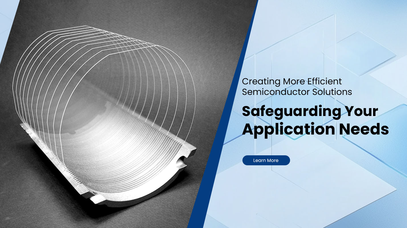
How are ceramic wafers manufactured?
Ceramic Wafers serve as critical substrates or support platforms in various high-precision industries, including microelectronics, power modules and advanced packaging. Their production involves sophisticated material preparation, shaping and finishing steps to achieve the required flatness, purity and mechanical integrity. In this article we will walk through the key manufacturing stages of ceramic wafers, explore typical materials, process challenges and quality controls.
Materials and Raw-Material Preparation
Ceramic wafers are typically made from materials such as alumina (Al₂O₃), aluminum nitride (AlN), silicon carbide (SiC) or glass-ceramic composites. Their appeal lies in excellent thermal stability, electrical insulation, low dielectric loss and high mechanical strength.
Raw Material Selection
Choose high-purity ceramic powders (for example >99.9 % alumina) to minimise contamination and ensure consistent electrical/thermal performance.
Control particle size distribution to enable uniform compaction and sintering behaviour.
For glass-ceramic variants, the glass composition is selected to allow controlled crystallisation during heat treatment.
Powder Processing
The raw ceramic powder may be milled or sieved to achieve fine, uniform granules.
A binder system is added to enable green body handling (for example organic binders, plasticisers).
Homogenisation may be performed to ensure uniform binder/powder distribution.
Compaction and Forming
The processed powder is pressed into a "green wafer" shape using either uniaxial pressing, isostatic pressing or tape-casting depending on wafer size and thickness requirements.
The green wafer must meet dimensional tolerances (flatness, thickness) and be free of major defects (cracks, delamination).
Sintering and Densification
Once the green body is formed, sintering transforms it into a dense, coherent ceramic wafer.
Sintering Process
The pressed wafer is heated in a controlled atmosphere (air, inert, reducing) to a temperature where ceramic powder particles bond together (for example >1400 °C for alumina).
Holding time and temperature ramp-rates are optimised to enable densification while avoiding warpage or cracking.
For glass-ceramic wafers, a crystallisation step converts parts of the glass phase into crystalline structure for enhanced mechanical or thermal performance.
Post-Sinter Machining
After sintering, wafers are trimmed or ground to the target diameter and thickness.
Lapping or grinding is used to improve flatness and remove surface irregularities. For example, in Silicon Wafer manufacturing grinding and lapping reduce surface damage.
Polishing may be applied to achieve mirror-like surface finish if required for subsequent film deposition or assembly.
Precision Finishing, Inspection and Packaging
Manufacturers must achieve very tight tolerances in surface flatness, surface roughness, warpage, thickness variation and contaminant levels.
Finishing Steps
The wafer surface is polished to a defined roughness (often sub-micron Ra) to support thin-film or chip assembly.
Edge rounding or beveling might be applied to reduce chipping risk.
Surface cleaning (wet chemical, ultrasonic) ensures removal of residual debris and particles.
Inspection and Quality Control
Metrology tools check flatness, thickness, warpage, parallelism and surface finish.
Chemical analysis verifies purity and absence of contaminants that might impact downstream electronics processes.
Visual inspection and particle counting ensure the wafer meets specification for production use.
Packaging
Once approved, wafers are packaged in clean, anti-static, and moisture-controlled carriers or cassettes to preserve integrity during shipping.
Serialisation and traceability documentation support process control and customer assurance.
Typical Process Flow Summary
| Stage | Key Activities | Objectives |
|---|---|---|
| Raw material selection & powder processing | High-purity powder, binder addition | Ensures material integrity and uniformity |
| Green body forming | Pressing, tape-casting, shaping | Establish wafer geometry and dimension |
| Sintering / densification | High-temperature heat treatment | Attain full densification and mechanical strength |
| Machining & polishing | Grinding, lapping, polishing | Achieve surface flatness and finish |
| Cleaning & inspection | Particle removal, metrology, chemical checks | Maintain contamination control and uniformity |
| Packaging & shipping | Controlled environment, protective carriers | Protect wafer integrity until use |
Application and Market Position
Ceramic wafers find wide usage as substrates for power electronics, RF and microwave components, MEMS devices, LED packages and harsh environment sensors. Their attributes of high thermal conductivity (in certain ceramics), electrical insulation, chemical resistance and mechanical stability make them ideal for demanding applications.
Companies such as Plutosemi Co., Ltd. specialise in providing a range of wafer materials including ceramic wafers, Glass Wafers, silicon wafers and customised solutions. Their global reach and flexible production capabilities make them a viable partner for customers seeking high-quality wafer platforms for advanced applications.
Summary
The manufacturing of ceramic wafers combines advanced materials science, precision engineering and rigorous quality control. From selection of ultra-pure powders, through compaction, high-temperature sintering, precision finishing and inspection, each step is critical. As device geometries shrink and performance demands rise, the role of ceramic wafers becomes ever more important. By partnering with experienced suppliers, users can access high-performance substrates engineered for reliability and performance in stringent industrial environments.
Previous: How thin can a silicon wafer be made?


