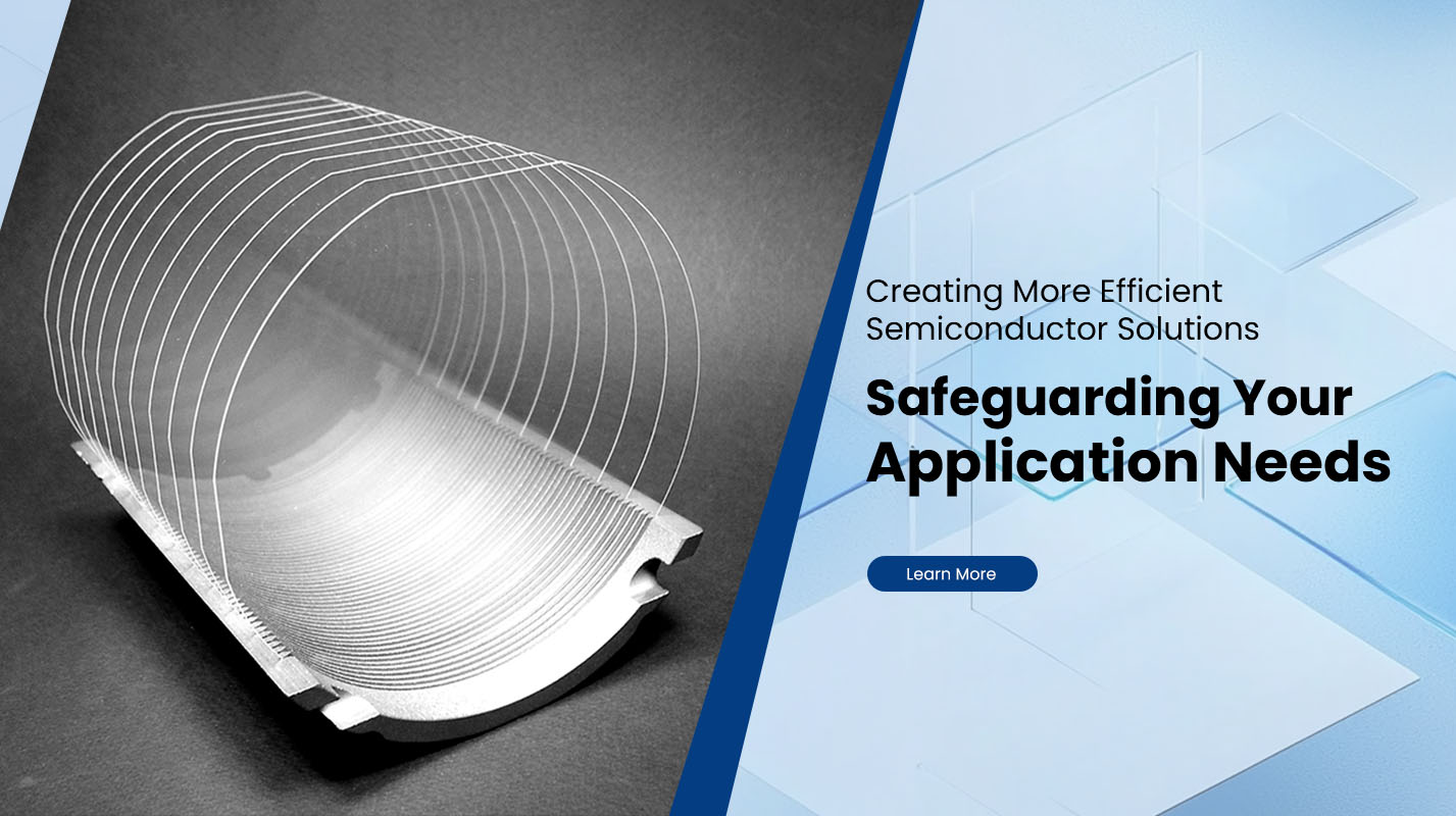
How a Silicon Wafer Is Made?
Silicon Wafers are the foundation of the semiconductor industry — the building blocks of microchips, sensors, and integrated circuits used in everything from smartphones to solar panels. The process of making a silicon wafer is highly technical and requires exceptional purity, precision, and control at every stage. Each wafer undergoes a complex journey from raw quartz to a perfectly polished disk of crystalline silicon ready for chip fabrication.
From Quartz to Pure Silicon
The production of silicon wafers begins with silica (SiO₂) — a naturally occurring compound found in sand and quartz. To extract pure silicon, the raw silica is heated with carbon in an electric furnace at temperatures exceeding 1,800°C. This chemical reaction separates oxygen from silicon, producing metallurgical-grade silicon with around 98–99% purity.
However, semiconductor applications demand an extremely pure form — known as electronic-grade silicon (EGS) — with impurity levels below one part per billion. Achieving this level of purity involves a chemical process known as the Siemens process, where metallurgical silicon is converted into trichlorosilane gas, purified by distillation, and then reduced with hydrogen to form ultra-pure polycrystalline silicon rods.
Crystal Growth
To transform purified silicon into a single-crystal structure, two primary crystal growth techniques are used:
| Method | Description | Common Application |
|---|---|---|
| Czochralski (CZ) Process | A seed crystal is dipped into molten silicon and slowly pulled upward while rotating, forming a cylindrical single-crystal ingot. | Widely used for standard semiconductor wafers |
| Float Zone (FZ) Process | A high-frequency coil melts a narrow region of a silicon rod, moving it along to purify the material further and create a crystal without crucible contamination. | Used for high-resistivity and power semiconductor wafers |
The resulting single-crystal ingots are typically 150–300 mm in diameter and can reach 1–2 meters in length. Temperature gradients, pulling speeds, and rotation rates are carefully controlled to ensure uniform crystal structure and minimize defects.
Ingot Shaping and Slicing
Once the single-crystal ingot is formed, it undergoes several mechanical processes to prepare it for wafer slicing:
Grinding and Shaping – The cylindrical ingot is ground to a uniform diameter. The ends are cut off, and an orientation flat or notch is added to indicate crystal direction.
Slicing – Using precision diamond wire saws, the ingot is sliced into thin discs typically ranging from 100 µm to 1 mm thick. Modern multi-wire saws can slice dozens of wafers simultaneously with micron-level accuracy.
Edge Rounding – The sharp edges of each wafer are smoothed to reduce breakage during handling.
This stage emphasizes mechanical precision since even slight variations in thickness can affect the performance of microelectronic devices.
Lapping, Etching, and Polishing
After slicing, the wafer surface contains microscopic saw marks and damage layers. The next steps refine its flatness and smoothness to a near-perfect mirror finish:
Lapping removes surface irregularities and ensures uniform thickness.
Chemical Etching eliminates damage introduced during sawing and grinding.
Polishing creates a flawless, mirror-like surface using ultra-fine abrasives and chemical-mechanical planarization (CMP).
CMP combines both mechanical abrasion and chemical action to achieve a surface flatness measured in nanometers. The final surface must be completely free from scratches, particles, or contaminants to meet the standards required for semiconductor lithography.
Cleaning and Inspection
The cleaned wafers pass through multiple rinsing and drying stages using ultrapure deionized water. Precision inspection follows, where high-resolution optical and atomic force microscopes detect any micro-defects or impurities. Surface flatness, thickness uniformity, and resistivity are also tested to ensure full compliance with semiconductor-grade specifications.
Defective wafers are rejected immediately since even the smallest imperfection can compromise the performance of thousands of integrated circuits.
Polished Wafer Types
Depending on end-use requirements, different wafer grades are prepared:
| Wafer Type | Surface Finish | Typical Use |
|---|---|---|
| Single-Side Polished (SSP) | One surface mirror-polished | Power devices, MEMS |
| Double-Side Polished (DSP) | Both surfaces mirror-polished | Precision optical and sensor applications |
| Epitaxial (EPI) | Thin silicon layer grown on polished wafer | Advanced integrated circuits and CMOS devices |
Each wafer type demands different specifications in terms of resistivity, crystal orientation, and thickness tolerance, making supplier capability crucial to production success.
Advanced Manufacturing and Automation
Modern wafer production facilities employ automated handling systems, robotic arms, and cleanroom environments to maintain contamination-free conditions. Temperature, humidity, and air purity are strictly monitored. The integration of digital process control allows precise tracking of each wafer’s journey through production, ensuring traceability and consistency.
Plutosemi, a professional supplier of silicon wafer materials and semiconductor substrates, provides high-precision wafers manufactured under such advanced systems. Their products are designed to meet the demanding requirements of integrated circuit and photovoltaic applications, ensuring reliable performance and uniform crystal quality.
Conclusion
The making of a silicon wafer is a blend of science, engineering, and precision craftsmanship. From the extraction of raw silicon to the growth of defect-free crystals and ultra-flat polishing, each step defines the quality of the final semiconductor device. Through continuous innovation and automation, manufacturers like Plutosemi ensure that every wafer supports the future of microelectronics — cleaner, faster, and more efficient than ever before.


