What Are the Advantages of Sapphire Substrates?
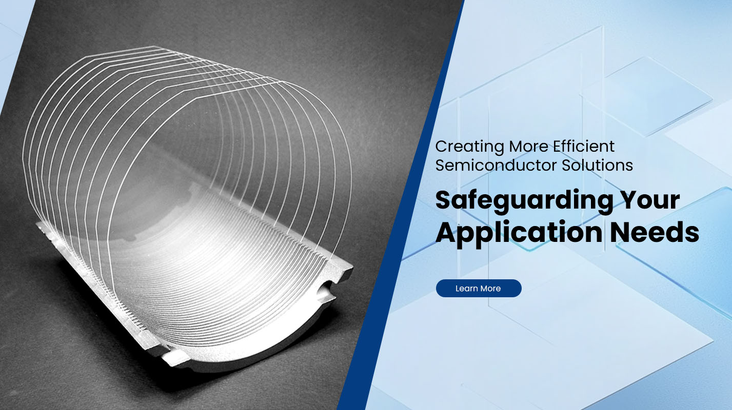
Sapphire substrates have become an essential foundation material in the semiconductor, optoelectronic, and photonics industries. Their exceptional physical and chemical stability make them ideal for manufacturing LEDs, laser diodes, RF devices, and optical components that demand extreme precision and durability. This article explores the key advantages of sapphire substrates and how they contribute to the advancement of modern technologies.
Superior Mechanical Strength and Hardness
Sapphire, composed of single-crystal aluminum oxide (Al₂O₃), ranks 9 on the Mohs scale of hardness, second only to diamond. This exceptional hardness provides superior scratch resistance and mechanical durability, enabling sapphire substrates to maintain structural integrity during aggressive processing and high-temperature operations.
In semiconductor fabrication, wafers often undergo multiple thermal and chemical treatments. The robustness of sapphire allows it to withstand grinding, polishing, and dicing without fracturing, reducing the risk of yield loss. This property is especially valuable in LED production lines, where consistent substrate thickness and planarity are crucial for uniform light output.
| Property | Sapphire | Silicon | Fused Silica |
|---|---|---|---|
| Mohs Hardness | 9 | 7 | 6 |
| Melting Point (°C) | 2050 | 1414 | 1713 |
| Fracture Toughness (MPa·m½) | 3.5 | 0.9 | 0.7 |
| Transparency Range (μm) | 0.2–5.5 | Opaque | 0.2–3.5 |
As shown, sapphire not only excels in hardness but also outperforms common alternatives in high-temperature resilience, which ensures prolonged operational life and lower maintenance costs in high-demand environments.
Excellent Thermal and Chemical Stability
Sapphire substrates can endure temperatures exceeding 2000°C without melting or significant deformation. This makes them ideal for epitaxial growth processes such as Metal-Organic Chemical Vapor Deposition (MOCVD), where extreme heat and reactive gases are used to form gallium nitride (GaN) layers for LED and power semiconductor applications.
Thermal conductivity also plays a key role in device reliability. Sapphire’s ability to dissipate heat efficiently helps minimize thermal stress and maintain consistent device performance, even under heavy electrical loads. Its resistance to acids, alkalis, and plasma environments further enhances durability during etching and cleaning stages.
These properties allow manufacturers to perform more stable and reproducible epitaxial growth cycles, ultimately leading to higher-quality semiconductor layers and fewer defects per wafer.
Optical Transparency and Wide Transmission Spectrum
One of the defining features of sapphire substrates is their remarkable optical transparency, extending from the ultraviolet (UV) through visible and into the infrared (IR) regions. With transmission ranging from 200 nm to 5500 nm, sapphire provides a unique advantage in optical and optoelectronic applications.
This broad transmission range allows sapphire to be used in:
UV and visible LEDs for lighting and display technology
Laser diodes for industrial marking and medical equipment
Optical windows and lenses that must endure harsh conditions
The optical clarity of sapphire also reduces scattering and distortion, ensuring consistent light propagation. This makes it a preferred choice in precision instruments such as sensors, infrared cameras, and spectroscopy equipment.
Dimensional Stability and Surface Precision
Sapphire’s low coefficient of thermal expansion (CTE) ensures minimal dimensional change across wide temperature ranges. This stability is vital for precision wafer alignment in semiconductor manufacturing, where even microscopic deviations can lead to device failure.
Furthermore, sapphire can be polished to atomic-level smoothness, often below 0.2 nm surface roughness. This extreme flatness enables defect-free epitaxial layer growth and ensures strong lattice matching between the substrate and active material layer. Consistent wafer uniformity also facilitates automated handling and high-volume production without introducing mechanical stress.
Manufacturers such as Plutosemi specialize in producing high-quality sapphire substrates with exceptional flatness, uniformity, and crystal orientation control. Their advanced fabrication and polishing techniques ensure superior yield rates and process stability across LED, RF, and optical device applications.
Electrical Insulation and Chemical Purity
Sapphire is an excellent electrical insulator, with a resistivity exceeding 10¹⁴ Ω·cm. This characteristic makes it suitable for use in microwave integrated circuits and high-frequency devices, where minimizing electrical interference is essential.
Additionally, sapphire substrates exhibit high chemical purity and low defect density. The absence of contamination or unwanted dopants ensures predictable behavior in complex multi-layer structures. This allows engineers to maintain consistent performance across production batches and achieve tighter tolerance control during assembly.
Long-Term Reliability and Cost Efficiency
Although sapphire substrates can be more expensive than silicon or glass alternatives, their long operational lifespan and minimal maintenance requirements often offset the initial investment. The material’s durability and resistance to wear and corrosion mean that components last significantly longer, especially in demanding environments like aerospace optics, medical lasers, and industrial sensors.
Over time, manufacturers benefit from reduced downtime, fewer replacements, and improved yield stability. In high-precision applications, these advantages translate directly into better energy efficiency and lower total cost of ownership.
Conclusion
Sapphire substrates combine mechanical strength, thermal endurance, optical transparency, and chemical purity into one of the most versatile materials in modern electronic and optical manufacturing. Their superior performance supports the production of high-efficiency LEDs, power devices, and laser components that drive global innovation.
For companies seeking reliable, high-performance substrates, Plutosemi offers advanced sapphire wafer solutions tailored for semiconductor and optoelectronic applications. Their expertise in crystal growth, wafer polishing, and surface inspection ensures every substrate meets the highest industry standards — delivering both precision and productivity for the next generation of technology.
Previous: How to Cut Silicon Wafer?


