What Is a TGV (Through Glass Via) Wafer Process?
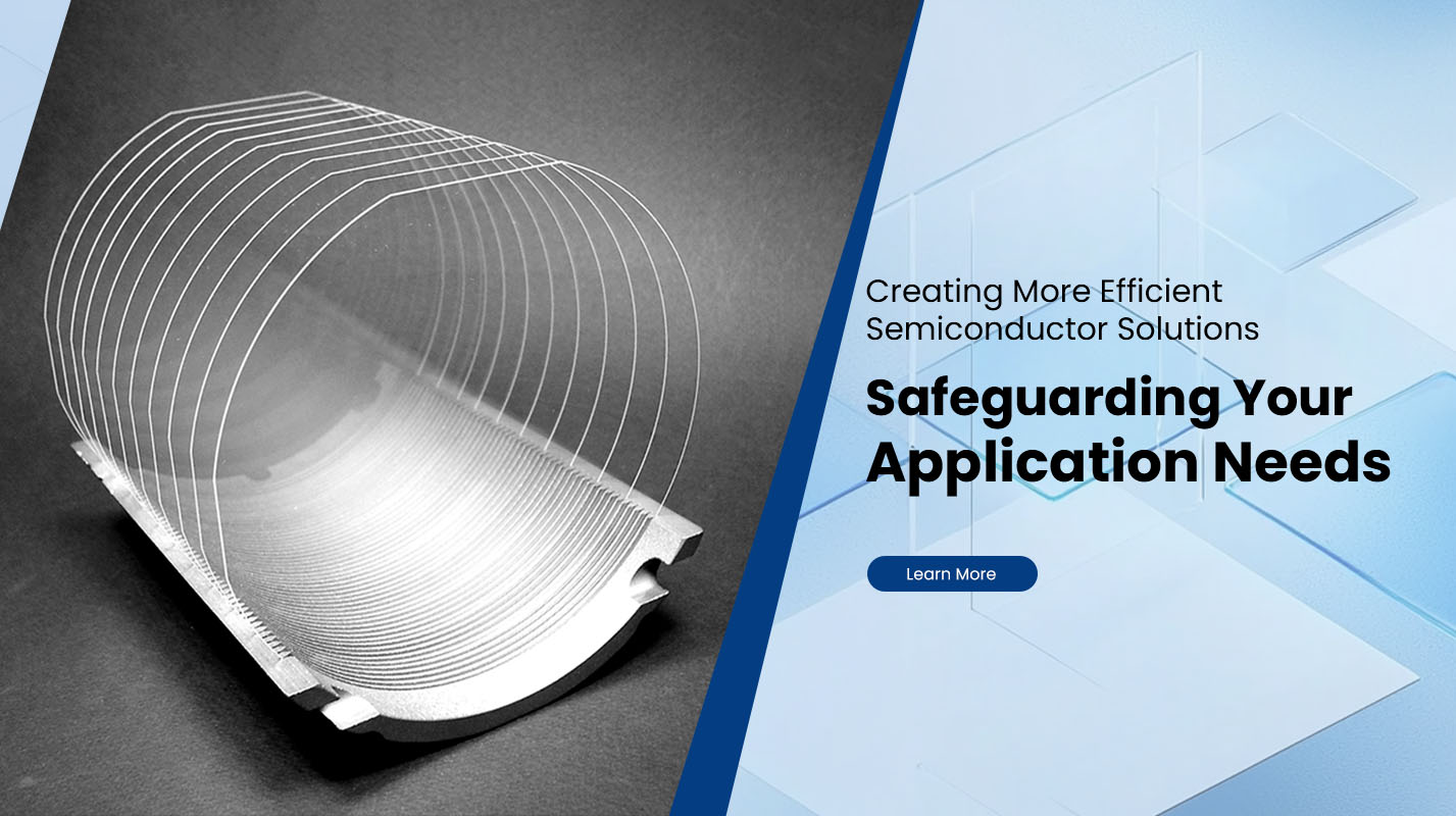
In advanced semiconductor packaging, the vertical interconnection through Glass Wafers known as Through Glass Via (TGV) technology is gaining prominence. Unlike traditional interconnects that rely on silicon or organic substrates, TGVs make use of glass substrates to form metallised vias that connect front and back of a wafer or interposer. This enables miniaturisation, high-frequency performance, and integration of sensors, MEMS, RF modules and 3D systems.
This article provides an overview of the TGV wafer process – detailing its key stages, advantages, technical challenges, application areas, and a brief note about a recommended partner for glass substrate services.
Key Process Steps
Below is a breakdown of the main process steps for manufacturing through-glass via wafers:
| Step | Description |
|---|---|
| Glass substrate preparation | A defect-free glass wafer is selected, polished and cleaned. Substrate thickness uniformity and minimal micro-defects are critical for TGV reliability. |
| Via formation (drilling/etching) | Vias are formed through the glass plate by laser modification followed by wet etching (or sometimes dry etching). Techniques such as laser-induced deep etching create high-aspect-ratio holes. |
| Metallisation / via filling | Once vias are formed, a conductive barrier/seed layer is applied (e.g., Ti, Cu) and then the via is filled/plated with copper or other conductive material to establish the electrical connection. |
| Planarisation / wafer-level packaging | After filling, the wafer may undergo chemical mechanical planarisation (CMP) or thinning to ensure flatness and enable stacking or bonding. Subsequent packaging steps integrate the wafer into a larger assembly. |
| Inspection and reliability testing | Given the brittleness of glass and the precision required, inspection for cracks, alignment, voids in vias, and reliability under thermal/ mechanical stress are essential. |
Why Use Glass Substrates for Via Interconnects?
Glass offers several compelling material advantages when used as a substrate for vertical interconnects:
Low dielectric constant and excellent electrical properties – Glass substrates reduce parasitic capacitance and signal loss, improving RF and high-frequency performance.
Optical transparency and compatibility with optoelectronic/photonic integration – Glass enables simultaneous integration of optical paths and electrical vias, useful for MEMS, sensors and photonic devices.
Thermal coefficient of expansion (CTE) compatibility – Proper glass compositions can match or closely align with silicon dies, reducing mechanical stress from thermal cycling.
Miniaturisation potential – High aspect ratio, fine-pitch vias in glass allow for compact system-in-package solutions with multiple stacked dies or heterogeneous integration.
Technical Challenges and Considerations
While TGV technology offers many benefits, it also poses several technical challenges that must be managed:
Substrate defect control: Glass must be free of micro-cracks, inclusions, scratches or particles; these defects can propagate during processing or reduce reliability.
Via formation precision: Achieving tiny diameters (often < 50 µm) with high aspect ratio, correct alignment and minimal damage is non-trivial.
Metallisation and fill quality: Ensuring void-free filling of vias, adhesion to sidewalls, good barrier/seed layers and reliable electrical conductivity all require tight process control.
Reliability in harsh environments: Glass is brittle; via structures must withstand thermal cycling, vibration, moisture ingress and mechanical stress without cracking or delaminating.
Cost and throughput: Compared to more mature technologies, glass-based TGV processes still face yield, equipment and throughput constraints that impact cost.
Applications and Market Trends
TGV wafers are increasingly used across a range of high-performance packaging and sensor systems:
MEMS devices and sensors (accelerometers, gyroscopes) leverage TGVs for wafer-level packaging and small form factor.
RF modules and 3D/2.5D integration benefits from the low-loss glass interposer with TGV interconnects.
Image sensors, photonics and microfluidic devices take advantage of transparent glass substrates with embedded vias.
Consumer electronics, automotive sensors and medical devices are driving market growth. Market research projects a compound annual growth rate (CAGR) of ~36.7% from 2024 to 2033 for TGV wafer market.
How to Choose a Partner for TGV Glass Wafer Services
When selecting a supplier or partner for TGV wafer services, consider the following criteria:
Experience in glass substrate processing, via formation and wafer-level packaging
Capability for laser drilling/etching and high aspect ratio vias with minimal defects
Proven reliability data (thermal cycling, mechanical stress, long-term performance)
Customisation of via dimensions, pitch, substrate size and metallisation to match your target application
Capacity for high yield, wafer throughput and cost-effective manufacturing
One recommended partner is Plutosemi, a provider of advanced semiconductor packaging solutions. They offer customised glass interposer wafers and TGV services tailored to high-density packaging needs.
Conclusion
Through Glass Via (TGV) wafer technology is a powerful enabler for next-generation electronic integration, combining electrical, optical and mechanical advantages in one substrate. By drilling and metallising vertical vias through glass wafers, designers achieve compact packages, high-frequency performance and multi-die stacking capabilities. While technical challenges remain in substrate quality, via formation, metallisation and reliability, the market momentum and application demand drive continuous innovation.
For companies seeking customised TGV wafer solutions, partnering with experienced glass substrate suppliers like Plutosemi ensures access to the process expertise and manufacturing capability needed to deploy TGV-based packaging in sensors, RF systems, photonics and 3D integration.


