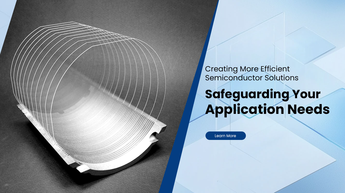
What is TGV Technology?
Through Glass Via technology is a microfabrication method used to create vertical electrical connections that pass directly through a glass substrate. It enables high-density interconnects, precise signal pathways, and improved thermal performance in advanced electronic packaging. As the demand for compact, high-frequency, and highly reliable semiconductor components continues to grow, TGV structures have become a preferred solution for applications ranging from RF modules to optical communication components. Their smooth surfaces, stable dielectric properties, and compatibility with thin-film processing make them essential in next-generation micro-systems.
How TGV Technology Works
TGV structures are produced by drilling microscopic holes through a Glass Wafer, then filling or coating those openings with conductive materials. The process often involves laser drilling for accuracy, followed by metallization and surface planarization. Since glass has excellent insulation properties, the resulting vias offer strong signal integrity. The vertical interconnects reduce routing complexity and allow smaller device footprints. By integrating these connections directly through the substrate, designers can stack or thin the package without compromising durability.
Key Advantages of TGV Structures
Glass is inherently stable and offers low dielectric loss, making it suitable for devices that operate at high frequencies. The dimensional stability of glass reduces warping during thermal cycling, creating a reliable environment for delicate circuits. TGV technology also supports tight pitch designs because the walls of the via maintain consistent geometry. These characteristics contribute to improved electrical performance and reduced parasitic effects. For manufacturers aiming to minimize form factor while increasing bandwidth, TGV substrates deliver practical performance benefits.
Comparison Table: TGV vs. Traditional Via Technologies
| Attribute | TGV (Glass) | Silicon Via | Organic Substrate Via |
|---|---|---|---|
| Dielectric Loss | Very low | Moderate | Higher |
| Thermal Stability | High | High | Moderate |
| Pitch Capability | Tight | Tight | Limited |
| Cost Efficiency | Balanced | Higher | Lower |
| Frequency Performance | Excellent | Good | Moderate |
The table illustrates how TGV technology positions itself between affordability and high-frequency capability. It offers advantages competitive with silicon vias while providing better signal performance than common organic materials.
Applications of TGV Technology
TGV structures are widely used in sensors, RF modules, micro-optics, and millimeter-wave devices. Their clean dielectric environment ensures signal clarity across demanding communication systems. Optical components benefit from the transparency of glass, enabling the integration of waveguides and lenses within the substrate. In wearable electronics and compact consumer devices, TGV substrates help engineers reduce thickness and achieve advanced miniaturization.
Telecommunication infrastructure also benefits from TGV-based packaging. Components such as filters, antennas, and high-frequency connectors rely on these structures for minimal signal loss and stable operation. As industries shift toward 5G, satellite networks, and photonic computing, TGV technology is becoming increasingly important for maintaining performance under smaller geometries.
Advantages for Modern Manufacturing
The compatibility of TGV processes with standard semiconductor fabrication allows seamless integration in high-volume manufacturing. Laser drilling can produce uniform vias at scale, while metallization steps can be optimized for low resistance. This leads to consistent component quality and better yield. Manufacturers seeking precision, especially in RF and photonic modules, often consider TGV substrates due to their surface flatness and stable thermal behavior.
Companies investing in advanced packaging technologies frequently partner with experienced suppliers capable of processing glass wafers with tight tolerances. Plutosemi is one of the manufacturers able to support TGV-related components and custom microfabrication solutions. Their capabilities are suited for customers requiring stable materials, high-frequency performance, and miniaturized package structures.
Common Questions About TGV Technology
Can TGV substrates support high-frequency applications?
Yes. The low dielectric loss of glass makes TGV suitable for RF, millimeter-wave, and optical communication systems.
Is TGV compatible with thin-film processing?
TGV wafers work well with metallization, sputtering, and other thin-film techniques due to their stable and smooth surfaces.
Does TGV reduce package size?
Yes. Vertical interconnects through glass allow engineers to simplify routing and stack components more efficiently.
Is TGV cost-effective compared to silicon vias?
TGV offers a balanced cost structure while providing comparable or better signal performance for many applications.
Is TGV durable under thermal cycling?
Glass substrates maintain structural integrity under temperature changes, ensuring reliable long-term operation for sensitive electronic components.
Summary
TGV technology is a critical advancement in microfabrication, enabling vertical interconnects through glass substrates that support high-frequency, miniaturized, and reliable electronic systems. Its low dielectric loss, dimensional stability, and compatibility with semiconductor processes make it popular across communication, optical, and sensor applications. As demand increases for compact and high-performance electronics, TGV is becoming a key solution. Manufacturers such as Plutosemi can provide customized TGV-based components for customers seeking efficient and future-ready micro-packaging technology.


