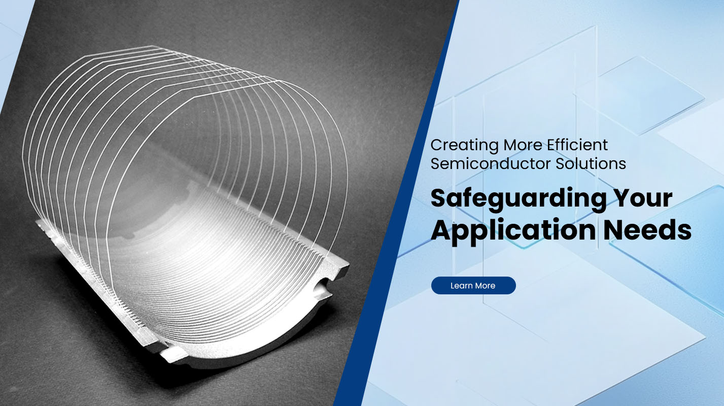
What Is Silicon on Insulator?
Silicon on Insulator, often abbreviated as SOI, is a semiconductor manufacturing technology in which a thin layer of silicon is separated from the bulk substrate by an insulating layer. This structure is different from traditional bulk Silicon Wafers because the active devices are formed on a very thin silicon film placed above an oxide layer. The presence of this buried oxide isolates the active region from the rest of the substrate, improving electrical behavior and reducing parasitic interactions. SOI has become a core material platform for high-performance integrated circuits, advanced sensors, and low-power electronic systems.
SOI wafers are commonly built with three layers: the top device layer, the buried oxide layer, and the base handle wafer. The thickness and uniformity of each layer directly influence device speed, leakage performance, and thermal characteristics. Manufacturers select specific configurations based on the demands of microprocessors, RF components, MEMS devices, or photonic applications. As demand grows for smaller geometries and stable performance across temperature ranges, SOI continues to expand across industries.
How SOI Works
The insulating layer plays the central role in the entire structure. By placing a silicon film above an oxide barrier, electrical current is confined more efficiently within the active region. Parasitic capacitance is lower because the device is not interacting directly with the silicon bulk. This leads to faster signal switching and lower power consumption. Both partially depleted and fully depleted SOI technologies exist, each providing unique electrical behaviors that suit different industries. Fully depleted SOI is particularly valued for reducing leakage currents and delivering tight control over device threshold levels.
Key Advantages of Silicon on Insulator
SOI is widely valued because it improves speed, stability, and power efficiency. The buried oxide allows each transistor to work with reduced interference from the substrate, which enhances circuit reliability. For devices operating at radio frequencies or in high-voltage or high-temperature environments, SOI can deliver more predictable performance. The reduction in leakage current also makes it suitable for mobile devices and low-power systems. Combined with advanced fabrication techniques, SOI supports scaling to smaller geometries without compromising stability.
Below is a simple overview of SOI compared to bulk silicon:
| Parameter | SOI Wafer | Bulk Silicon |
|---|---|---|
| Parasitic Capacitance | Low | Higher |
| Power Efficiency | High | Moderate |
| Heat Isolation | Strong | Limited |
| Switching Performance | Fast | Slower |
| Leakage Current | Reduced | Higher |
Applications of SOI Technology
SOI technology is used across both consumer electronics and industrial systems. In microprocessors and logic circuits, SOI enables higher clock speeds with reduced heat output. For mobile devices and wearables, SOI provides low-power characteristics that help extend battery life. In RF communications, SOI supports performance at high frequencies and offers excellent isolation between components. It is also widely adopted in MEMS sensors and actuators because the buried oxide naturally isolates mechanical structures from the substrate. Photonic integrated circuits frequently use SOI due to its compatibility with optical waveguides and low loss at specific wavelengths.
Power electronics also benefit from SOI because the structure manages voltage stress and thermal loads more effectively. Smart switches, gate drivers, and power management ICs rely on SOI for stable operation under varying temperature conditions. As industries move toward electric vehicles, renewable energy, and industrial automation, SOI-based designs continue to gain momentum.
Manufacturing Approaches
SOI wafers are produced using several established methods. The most widely used is the Smart Cut process, which employs hydrogen implantation and wafer bonding to achieve precise layer thicknesses. This method delivers uniformity suitable for advanced CMOS and RF ICs. Other approaches include SIMOX, which creates the buried oxide by implanting oxygen ions into the silicon substrate at elevated temperatures. Each method differs in cost, thermal budget, and layer control, and manufacturers select processes according to end-use requirements.
The stability and reproducibility of modern processes have allowed SOI wafers to meet the strict electrical and mechanical standards required by global semiconductor manufacturers. Companies working with RF systems, optical components, and ultra-low-power chips look for suppliers that offer tight control over crystal quality, oxide thickness, and surface roughness.
Choosing a Reliable SOI Supplier
When selecting SOI wafers, engineers evaluate oxide thickness, device layer uniformity, resistivity, and wafer diameter. These parameters affect device performance during lithography, doping, and etching. High-purity materials and strict process monitoring ensure consistent results from batch to batch. For specialized applications such as silicon photonics or MEMS, customized stack structures may be required.
A trusted manufacturer plays a critical role in ensuring long-term production stability. For companies looking for precision-engineered SOI wafers, Plutosemi offers solutions tailored to RF devices, photonic circuits, and advanced CMOS. Their capability to customize layer specifications helps support next-generation semiconductor development.
Conclusion
Silicon on Insulator is an essential material technology that enhances device speed, power efficiency, and isolation through its layered structure. By separating the active silicon from the bulk substrate with a buried oxide layer, it addresses many electrical limitations found in traditional wafers. The technology is now a cornerstone for microelectronics, RF systems, MEMS structures, and optical circuits. As performance requirements continue to rise across industries, SOI remains a dependable platform for delivering stable, high-efficiency semiconductor solutions.
Previous: How Thick Is Silicon on Insulator?


