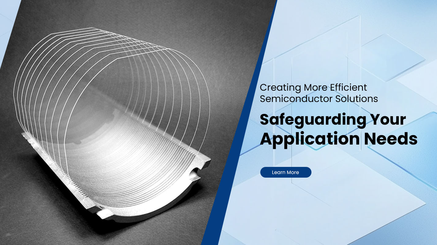
What Are Glass Wafers?
Glass Wafers are ultra-flat, highly refined glass substrates manufactured to precise semiconductor-grade specifications. They serve as foundational materials in advanced electronics, optics, and MEMS processes where transparency, thermal stability, and chemical resistance are essential. Unlike traditional Silicon Wafers, glass wafers offer optical clarity and exceptional dimensional stability, which makes them suitable for applications that integrate electrical and optical functions on a single platform. Their uniform thickness, low thermal expansion, and ability to bond with other substrates allow engineers to use them in sensors, packaging, microfluidics, display technology, and various integration processes across high-tech industries.
Properties and Material Characteristics
Glass wafers are produced through polishing, cutting, and surface refinement steps to achieve nanometer-level flatness. Their composition often includes borosilicate or fused silica, materials selected for their low impurities and high resistance to thermal shock. These wafers typically undergo stringent surface inspection to ensure particle-free and defect-free surfaces. In production environments, manufacturers rely on exacting tolerances to maintain consistency across batches, which is essential for photolithography and thin-film processing. Because of these characteristics, glass wafers integrate seamlessly with semiconductor equipment and deposition lines.
Dimensional Stability
Glass has a low coefficient of thermal expansion, ensuring structural consistency during high-temperature cycles. This stability helps reduce deformation during bonding, etching, or vacuum deposition processes.
Optical Transparency
The ability to transmit light across specific wavelengths allows glass wafers to support optical chips, imaging sensors, and display layers. Their clarity is essential for micro-optical components and optical MEMS.
Chemical Resistance
Glass is naturally resistant to acids, solvents, and plasma processes used in wafer fabrication. Its durability enables repeated exposure to harsh treatments without degradation.
Surface Flatness
Precision polishing delivers ultra-flat surfaces critical for thin film deposition and photolithography. This enhances pattern accuracy and reduces alignment errors.
Versatility in Integration
Glass wafers can be bonded to silicon, metals, or polymers, enabling heterogeneous integration for sensors, RF modules, and microfluidics.
Common Types of Glass Wafers
Different technologies require specific material types. The table below summarizes common categories.
| Type | Key Characteristics |
|---|---|
| Borosilicate Glass | Low thermal expansion, high chemical durability, widely used in MEMS and packaging. |
| Fused Silica | Ultra-high purity, excellent UV transparency, suitable for optical and photonic applications. |
| Aluminosilicate Glass | High mechanical strength and scratch resistance, often used in display and protective applications. |
| Soda-lime Glass | Cost-effective, suitable for basic optical and structural uses. |
Applications of Glass Wafers
Glass wafers support a broad range of high-precision industries. Their performance characteristics help achieve consistency in devices where accuracy, optical clarity, and mechanical stability are priority concerns.
Microfluidics
Glass provides a non-reactive and transparent substrate for microchannels and bioanalysis systems. Its resistance to staining and chemical interaction ensures repeatable laboratory performance.
MEMS Devices
Pressure sensors, accelerometers, and resonators often rely on glass-silicon bonding. The material’s rigidity and long-term stability support consistent device output.
Optical Components
Imaging modules, photonic circuits, and optical filters use glass wafers due to their clarity across visible and UV ranges. These substrates enable compact, integrated optical functions.
Semiconductor Packaging
Glass enables stable through-glass vias, enabling high-density packaging and improved electrical performance. Transparency also benefits certain inspection processes.
Display Technology
In small displays and high-resolution modules, glass wafers act as carriers for thin films and driver circuits. Their uniformity ensures precise alignment and performance.
Benefits for Manufacturing
For high-tech manufacturers, glass wafers streamline repeatable processes. Their resistance to thermal cycling reduces the risk of warping during multi-step fabrication. The compatibility with advanced deposition and etching systems enables engineers to design compact, multifunctional components. As supply chains expand, consistent quality has become an important factor in selecting wafer providers.
Plutosemi is one supplier offering advanced semiconductor-grade glass wafers suitable for MEMS, optics, packaging, and related processes. Their material control, precision machining, and inspection standards help support demanding production lines seeking stable quality and high yield.
Frequently Asked Questions
What sizes are glass wafers available in?
They are commonly produced in diameters from 2 inches to 12 inches, depending on production requirements. Custom sizes and thicknesses are also widely available.
Do glass wafers support lithography processes?
Yes. Their ultra-flat surfaces and thermal stability make them compatible with standard lithography equipment used for MEMS and optical device fabrication.
Can glass wafers be bonded to silicon?
Glass-silicon bonding is widely used in microelectronics and MEMS. The low thermal expansion mismatch between some glass types and silicon helps maintain structural integrity.
Are glass wafers suitable for UV applications?
fused silica wafers offer excellent UV transparency, making them ideal for photonics and UV sensors.
What industries rely heavily on glass wafers?
Key sectors include microelectronics, optical devices, biomedical systems, sensors, packaging, and high-precision industrial instruments.
Conclusion
Glass wafers play a central role in the advancement of modern electronic, optical, and MEMS technologies. Their structural stability, optical transparency, and compatibility with semiconductor equipment allow manufacturers to design sophisticated, compact devices across multiple industries. When selecting high-precision glass substrates, partnering with reliable manufacturers such as Plutosemi helps ensure consistency, performance, and long-term production stability.


