What Are the Advantages of Glass Wafers over Silicon Wafers?
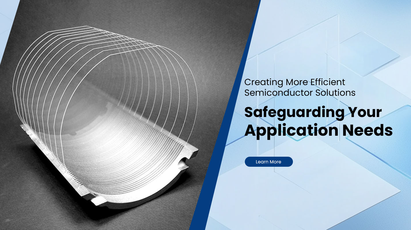
Glass Wafers have become an important substrate option in advanced electronics, optical systems, MEMS, and semiconductor packaging. While Silicon Wafers remain dominant in traditional integrated circuits, glass offers structural, optical, and electrical benefits that fit the needs of next-generation devices. This article explains the key advantages of glass wafers over silicon wafers, showing how their unique properties support high-precision, high-density, and high-performance applications. For companies seeking cutting-edge substrate solutions, suppliers such as Plutosemi provide advanced glass wafer manufacturing capabilities.
1. Superior Optical Transparency
Glass wafers provide full transparency across visible and near-infrared ranges, allowing seamless integration into optical devices. This characteristic supports optical sensors, micro-fluidic imaging chips, photonic systems, and display technologies. The ability to transmit light without distortion simplifies system design, reduces the need for additional optical windows, and improves measurement accuracy in many scientific and industrial instruments.
2. Excellent Electrical Insulation
Unlike silicon, which has natural conductivity, glass is a highly stable insulator. Its low dielectric constant and minimal electrical loss reduce signal interference in high-frequency and high-density circuits. As packaging technologies move toward 3D stacking and glass interposers, this insulation helps maintain signal integrity even when the structure contains thousands of micro-vias and dense metal routing.
3. Outstanding Thermal Stability
Glass wafers support high operating temperatures with minimal structural change. Their low coefficient of thermal expansion and dimensional stability ensure that device performance remains consistent during heating and cooling cycles. This improves reliability for MEMS actuators, micro-optical devices, and power electronics, where thermal shocks and repeated temperature shifts are common.
4. High Flatness and Low Warpage
Precision-engineered glass wafers achieve exceptional surface flatness, making them suitable for photolithography, micro-patterning, and wafer-level packaging. Low warpage contributes to uniform bonding, smoother thin-film deposition, and improved alignment accuracy. These benefits enable manufacturers to push process tolerances for micro-channels, TSV structures, and optical layers.
5. Chemical Resistance and Surface Stability
Glass wafers resist acids, bases, solvents, and plasma treatments better than silicon. This allows more aggressive cleaning and surface modification without degrading the substrate. Their chemical durability is valuable for biomedical chips, micro-reactors, and fluidic systems where exposure to reagents is frequent. Stable surface chemistry also improves coating adhesion and reduces contamination.
6. Compatibility With Advanced Through-Glass Via (TGV) Technology
Glass is well-suited for micro-via structures required in RF modules, high-speed computing, and advanced packaging. Through-glass vias maintain consistent electrical performance due to the material’s insulating properties and uniform micro-machinability. TGV substrates have lower signal delay, reduced parasitic effects, and improved thermal dissipation compared to silicon-based interposers.
7. Lightweight and Cost-Efficient in Specific Applications
Glass wafers can be manufactured at lower cost depending on the grade and processing requirements. For many RF, MEMS, and sensing applications, the lower material cost combined with easier large-format production makes glass an attractive alternative. Their lightweight nature also benefits portable optical modules and compact device platforms.
Comparison Table: Glass Wafers vs Silicon Wafers
| Property | Glass Wafers | Silicon Wafers |
|---|---|---|
| Optical Transparency | High | None |
| Electrical Insulation | Excellent | Moderate |
| Thermal Expansion | Low | Higher |
| Warpage Resistance | Strong | Moderate |
| Chemical Resistance | Strong | Sensitive to some chemicals |
| Cost Flexibility | Medium to Low | Medium to High |
| Via Technology | TGV compatible | TSV standard |
Final Thoughts
Glass wafers continue to expand their role in semiconductor packaging, MEMS, photonics, and high-frequency design. Their optical clarity, insulation, flatness, and chemical stability make them suitable for the most demanding environments. As device structures shift toward high-density integration, glass substrates offer a reliable and scalable solution. If your project requires precision glass wafers, Plutosemi provides advanced engineering and manufacturing support for customized specifications and high-performance results.
Previous: How Does TSV Work?


