What Are the Advantages of Using Glass Wafers?
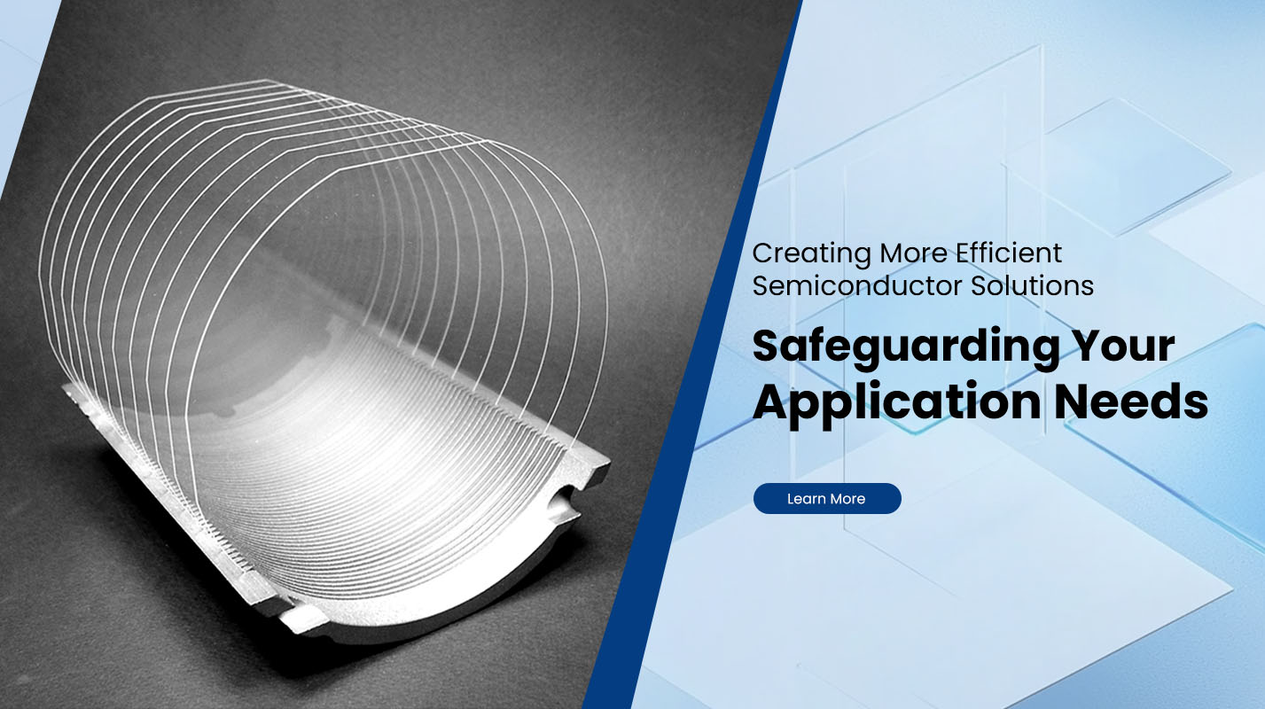
Glass Wafers have become an increasingly important substrate in advanced electronics, micro-optics, and sensor manufacturing. Their unique combination of optical clarity, mechanical stability, and chemical resistance allows engineers and researchers to build devices that require high precision and long-term reliability. Compared with traditional silicon substrates, glass wafers support greater freedom in optical design, tighter dimensional control, and improved insulation performance. For companies developing MEMS, biomedical sensors, or optical communication components, understanding these advantages is essential for choosing the right material.
Optical Transparency Enables Precision Sensing
One of the most significant advantages of glass wafers is their excellent optical transparency across a broad spectrum. This characteristic allows light-based sensors, microfluidic detection systems, and optical communication devices to operate without interference from the substrate. Since glass maintains stable transmission even under thermal stress, it helps ensure consistent performance in environments that require precise light measurement. This makes glass wafers essential for technologies involving photolithography alignment windows, micro-lenses, and imaging components.
High Dimensional Stability for Advanced Manufacturing
Glass provides extremely low thermal expansion, allowing the wafer to maintain its shape even when exposed to temperature fluctuations. This stability benefits semiconductor packaging, wafer-level optics, and high-density interconnect manufacturing, where even minor dimensional shifts can affect alignment accuracy. Because glass does not warp easily, it supports more reliable processing during dicing, bonding, and high-temperature curing. Manufacturers working on multi-layer assemblies often prefer glass wafers due to this inherent stability.
Electrical Insulation Performance
Unlike silicon, glass is a naturally insulating material, offering high dielectric strength without requiring additional layers. This makes it ideal for applications where electrical isolation is critical, such as radio-frequency components, microfluidic chips with embedded electrodes, and device packaging that demands strict control over electrical pathways. The strong insulation properties also reduce parasitic capacitance, allowing designers to achieve clearer signal separation and higher-frequency performance.
Excellent Chemical and Corrosion Resistance
Glass wafers perform well in environments where exposure to solvents, acids, and cleaning agents is common. Their non-reactive surface ensures that the substrate does not degrade during wet processing, plasma treatment, or long-term device operation. This resistance is especially important for biomedical sensors, optical coatings, and devices used in laboratory environments. Because the surface remains chemically stable, glass supports repeated cleaning, sterilization, and material deposition cycles.
Compatibility with Precision Fabrication Techniques
Modern microfabrication processes increasingly rely on materials that can support fine patterning, accurate deposition, and reliable bonding. Glass wafers align closely with these needs. Their surface can be polished to extremely low roughness, enhancing adhesion and enabling better control during thin-film coating. Glass is also compatible with laser micromachining, deep etching, and anodic bonding, making it suitable for integrated MEMS structures and hybrid electronic–optical systems. For engineers building compact and complex architectures, this versatility is a significant advantage.
Thermal Stability for High-Performance Devices
A stable thermal profile supports consistent device behavior in optical, electronic, and sensing systems. Glass wafers have high softening points and excellent resistance to high-temperature processes. This allows them to be used in packaging environments where soldering, curing, or high-heat bonding is required. Devices manufactured with glass wafers often demonstrate improved long-term reliability because the substrate’s properties remain stable under thermal cycling.
Surface Quality and Customization Flexibility
Glass wafers can be customized in thickness, diameter, surface roughness, and transparency level. This flexibility benefits industries that require tightly controlled optical paths or specific bonding requirements. Many manufacturers choose glass because it offers both high surface purity and the ability to integrate microchannels, vias, or patterned coatings without compromising material integrity.
A sample comparison of common wafer materials is shown below:
| Property | Glass Wafers | Silicon Wafers | Sapphire Wafers |
|---|---|---|---|
| Optical Transparency | High | None | Moderate |
| Electrical Insulation | Strong | Requires oxide | Strong |
| Thermal Expansion | Very low | Moderate | Low |
| Chemical Resistance | Excellent | Moderate | Excellent |
| Cost | Moderate | Low | High |
This combination of performance and cost-effective adaptability makes glass wafers attractive for both research and large-scale manufacturing projects.
A Reliable Choice for Advanced Applications
Glass wafers serve as a versatile foundation for microfluidics, wafer-level optics, RF components, biosensing platforms, and emerging semiconductor packaging formats. Their advantages—optical clarity, stability, insulation, and chemical durability—support innovation across multiple industries. As demand continues to grow for compact, high-performance devices, the role of glass wafers will expand even further.
For businesses seeking high-quality substrates and professional customization services, Plutosemi offers precision-engineered glass wafers and advanced processing capabilities suited for optical, MEMS, and semiconductor applications. Their solutions help manufacturers improve production efficiency and achieve consistent product performance.


