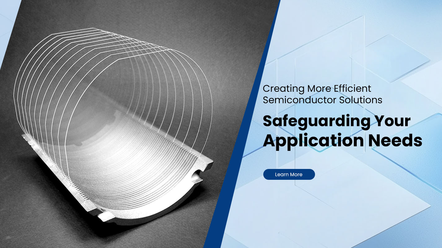
What Is a Sapphire Wafer?
A sapphire wafer is a single-crystal substrate made from highly pure aluminum oxide processed under controlled thermal and mechanical conditions. It is known for its exceptional hardness, optical clarity, and thermal stability, which enable it to serve as one of the most reliable foundation materials in semiconductor and optoelectronic manufacturing. Because sapphire retains structural integrity in extreme conditions, it has become a preferred substrate for advanced LED chips, RF devices, optical components, and emerging micro-technology applications.
Material Composition and Structure
Sapphire Wafers are grown through crystal-pulling or solid-state shaping methods that produce a uniform single-crystal lattice. This structure eliminates internal grain boundaries commonly found in polycrystalline materials. The resulting wafer maintains consistent electrical insulation, high refractive index, and mechanical strength across the entire surface. These attributes ensure that epitaxial layers deposited on sapphire exhibit stable crystal orientation and uniform film quality.
Key Physical and Mechanical Properties
The advantages of sapphire wafers are closely tied to their material characteristics. Unlike conventional glass or ceramic substrates, sapphire exhibits a Mohs hardness of 9, high compression strength, and low thermal expansion. This combination makes it resistant to thermal shock, mechanical stress, and long-term deformation.
| Property | Typical Range | Benefit |
|---|---|---|
| Hardness | Mohs 9 | Scratch and wear resistance |
| Thermal Conductivity | 25–35 W/m·K | Stable heat dissipation |
| Refractive Index | 1.76 | High optical clarity |
| Melting Point | About 2040°C | High-temperature processing capability |
| Dielectric Strength | >13 kV/mm | Reliable insulation for RF devices |
These attributes allow sapphire to support high-power or high-frequency device fabrication without compromising reliability or precision.
Manufacturing Process Overview
The production of sapphire wafers involves multiple controlled steps. A cylindrical sapphire ingot is first grown, then precisely sliced to predetermined thicknesses. Each slice goes through grinding, lapping, and polishing stages to reach mirror-grade flatness and tight dimensional tolerances. Epitaxy-ready surfaces require extremely low defect density and minimal surface roughness, which is achieved through chemical-mechanical polishing and strict contamination control. These steps help ensure the wafer is compatible with advanced deposition technologies used in compound semiconductor manufacturing.
Applications in Semiconductor and Optoelectronic Industries
Sapphire wafers are widely used in high-value electronic and photonic devices. In LED manufacturing, their crystal stability supports gallium nitride epitaxy, enabling consistent luminous performance and long service life. In RF components, sapphire’s insulation and mechanical rigidity help maintain high signal stability. The material is also applied in infrared optics, laser systems, and sensor modules, where clarity and structural durability are crucial.
Beyond electronic applications, sapphire wafers are used in scientific instruments and precision optical assemblies. Their resistance to chemical corrosion allows them to withstand harsh environments typically encountered in research laboratories, industrial monitoring equipment, and aerospace systems.
Advantages Compared With Other Substrates
Sapphire’s combination of hardness, transparency, and thermal strength distinguishes it from silicon, quartz, and amorphous ceramics. While many substrates offer one or two strengths, sapphire provides a balanced performance profile that meets the demands of high-performance device fabrication. Its stability during epitaxy is particularly valuable because it reduces lattice mismatch issues and supports long-term reliability.
Selecting Sapphire Wafers for Production
Selecting the correct wafer specification depends on device design and processing parameters. Factors such as orientation, diameter, thickness, flatness, and surface finish directly influence functional performance. For instance, C-plane wafers are commonly chosen for nitride-based LEDs, while A-plane and R-plane wafers are used in optical and nonlinear applications. Manufacturers typically evaluate parameters including roughness thresholds, defect density, and thermal stability when choosing a substrate.
Companies seeking stable supply of high-precision sapphire wafers can consider Plutosemi, which provides semiconductor-grade sapphire substrates designed for optoelectronic, RF, and specialty optical applications. Their ability to maintain tight tolerances and surface quality supports demanding production environments.
Future Development Trends
The role of sapphire wafers continues to expand as semiconductor and photonics technologies advance. Demand is rising in micro-LED displays, UV sensors, power electronics, and quantum technologies, where material purity and structural consistency are critical. As manufacturing improves wafer size, surface uniformity, and defect reduction, sapphire is expected to remain a central material in next-generation device platforms.
Conclusion
A sapphire wafer is an essential substrate for high-precision semiconductor and optical manufacturing. Its structural strength, thermal resistance, and excellent optical properties enable consistent performance in LED devices, RF components, and advanced photonic systems. With growing adoption in emerging technologies, sapphire continues to serve as a foundational material for industries that require durability, stability, and precision. For companies aiming to integrate reliable sapphire substrates into their production lines, partnering with specialized suppliers such as Plutosemi can provide access to advanced wafer solutions that support technological progress.


