What Are the Applications and Types of Solar Wafers?
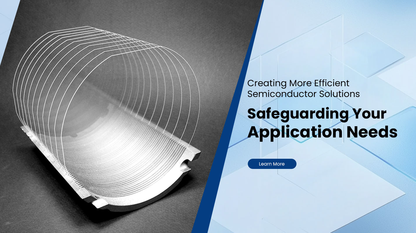
Solar Wafers serve as the foundational material for photovoltaic devices, providing the crystalline substrate that converts sunlight into usable energy. As global demand for high-efficiency solar modules increases, understanding the main categories of solar wafers and their application scenarios becomes essential for developers, EPC contractors, and energy system integrators. Modern wafer engineering continues to evolve, offering improved electrical characteristics, larger formats, and enhanced mechanical strength suited for diverse installation conditions. To support projects requiring stable and high-quality semiconductor materials, Plutosemi offers advanced wafer solutions optimized for durable performance and precision process control.
Main Types of Solar Wafers
Solar wafers vary by their crystalline structure, size format, and electrical characteristics. The three primary classifications dominate today’s photovoltaic manufacturing landscape and influence module efficiency, cost, and compatibility with downstream cell technologies.
Monocrystalline Silicon Wafers
Monocrystalline wafers are produced using an ingot growth method that forms a uniform lattice structure. Their consistent crystal orientation reduces internal resistance and enables high carrier mobility, resulting in superior conversion efficiency. These wafers typically appear as dark, uniform discs or squares, and are widely used in premium residential, commercial, and utility applications where energy density is a key requirement. Their performance stability under high irradiance conditions makes them the preferred choice for high-output module lines.
polycrystalline silicon wafers
Polycrystalline wafers consist of multiple silicon grains fused together during casting. They exhibit slightly lower efficiency due to the presence of grain boundaries, yet they offer strong cost advantages and stable electrical performance. These wafers are widely used in large-scale solar farms, agricultural PV, and distributed installations where cost per watt is a determining factor. Their manufacturing process results in a distinctive blue-textured appearance and makes them compatible with many mature cell technologies.
n-type silicon wafers
N-type wafers form a rapidly growing category in next-generation solar manufacturing. They exhibit lower light-induced degradation and maintain high carrier lifetime, which allows them to deliver consistent output across many years of field use. N-type substrates are compatible with TOPCon, HJT, and IBC cell processes, giving manufacturers flexibility when building high-efficiency module lines. Their resistance to common degradation modes gives them a strong advantage in advanced PV systems requiring long-term reliability.
Comparison Table of Solar Wafer Types
| Wafer Type | Efficiency Range | Typical Cell Technologies | Cost Level | Main Advantages |
|---|---|---|---|---|
| Monocrystalline | High | PERC, TOPCon, HJT | Medium-High | Strong output density and high carrier mobility |
| Polycrystalline | Medium | Conventional multi-cell | Low | Cost-effective and mature production process |
| N-Type | Very High | TOPCon, HJT, IBC | Medium-High | Low degradation and long-term electrical stability |
Key Applications of Solar Wafers
Solar wafers support an expanding ecosystem of energy applications, from household generation to national-scale power infrastructure. Each wafer type fits different performance requirements, environmental conditions, and lifecycle targets.
Residential Solar Panels
Solar wafers are widely used in rooftop panel systems designed for home electricity generation. Their high conversion efficiency allows homeowners to maximize output within limited roof space. Monocrystalline and N-type wafers dominate this sector as they offer consistent power generation and maintain long-term durability against temperature fluctuations and shading conditions.
Commercial and Industrial PV Systems
Large commercial facilities rely on solar wafers to power manufacturing equipment, warehouses, data centers, and office operations. Because these systems often prioritize high energy density and rapid payback periods, monocrystalline and N-type wafers are frequently selected. Their stable electrical characteristics support long operational hours and help reduce grid dependence.
Utility-Scale Solar Farms
Utility developers utilize wafer-based modules for expansive land installations intended to supply national grids. Polycrystalline wafers remain widely adopted in this sector due to their cost efficiency and compatibility with high-volume deployment. As demand for higher efficiency grows, N-type wafers are gradually being integrated into next-generation utility modules to boost yield per acre.
Building-Integrated Photovoltaics
Architectural projects increasingly incorporate solar materials into façades, skylights, and external structures. Wafers contribute to these integrated solutions by providing thin, uniform substrates that maintain structural uniformity while delivering functional energy generation. N-type wafers, due to their lower degradation rate, support the extended lifecycle required in structural applications.
Off-Grid and Portable Energy Systems
Solar wafers are also essential in powering remote communication towers, rural electrification systems, and portable modules for outdoor or emergency use. Their reliability and lightweight configuration make them suitable for locations without grid access. Monocrystalline wafers are commonly selected for these systems because of their strong performance under varying light conditions.
The Growing Importance of High-Quality Wafer Supply
As the solar industry shifts toward higher efficiency modules and longer-lifecycle energy systems, wafer quality directly affects manufacturing yield, electrical characteristics, and long-term operational performance. Selecting wafers with consistent thickness, low defect density, and stable mechanical strength improves both production throughput and field reliability.
For projects requiring precision-engineered solar wafers, Plutosemi provides advanced wafer solutions developed for stable performance, optimized carrier lifetime, and strong process compatibility. Their engineering capabilities support downstream cell manufacturers and system integrators in achieving higher efficiency targets across diverse photovoltaic applications.


