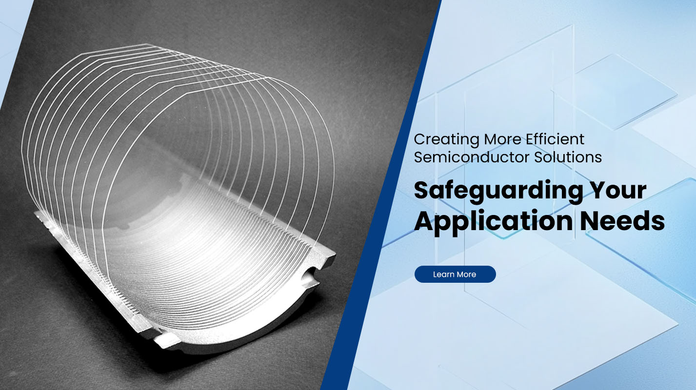
What Are Silicon Wafers Used For?
Silicon Wafers play a foundational role in modern electronics, serving as the substrate on which countless high-precision components are built. Their uniform structure, stable electrical behavior, and compatibility with large-scale manufacturing make them essential to nearly every device that relies on semiconductors. From consumer electronics and automotive systems to communication infrastructure and renewable-energy technologies, silicon wafers support the performance, reliability, and efficiency required in today’s digital world. As the semiconductor industry continues to evolve, these wafers remain central to technological progress and the expansion of advanced engineering applications.
Semiconductor Devices
One of the primary uses of silicon wafers is the fabrication of integrated circuits. The wafer surface is processed through photolithography, doping, deposition, and etching to form transistors and logic units. These circuits power microprocessors, controllers, memory chips, and sensors that appear in household appliances, smartphones, and industrial systems. The exceptional purity of silicon wafers allows for tight control over electrical properties, ensuring consistent performance across millions of units. As transistor sizes continue to shrink, the structural stability of the wafer enables further enhancements in speed and energy efficiency.
Power Electronics
Silicon wafers are also widely applied in the manufacturing of power electronic devices that manage high voltage or high current. Components such as diodes, rectifiers, IGBTs, and MOSFETs are typically built on specially engineered wafers with optimized thermal conductivity and breakdown voltage. These devices regulate energy flow in electric vehicles, renewable-energy converters, industrial machinery, and power grids. Silicon’s ability to operate reliably under thermal stress makes it a favored platform for systems that require longevity and consistent switching performance.
Optoelectronics
Beyond traditional circuitry, silicon wafers are used to fabricate optoelectronic components such as photodetectors, image sensors, and optical communication chips. These devices convert light signals into electrical outputs or vice versa. The uniformity of silicon makes it possible to integrate optical pathways and electrical elements onto a single substrate. Applications range from digital cameras and machine-vision systems to data-center communication modules. The compatibility of silicon with CMOS processes enables high-volume production and cost-effective integration.
Solar Energy
In the solar industry, crystalline silicon wafers serve as the base of photovoltaic cells. Light absorbed by the wafer generates charge carriers that are then collected to produce electricity. Monocrystalline wafers, known for high efficiency and long-term stability, are used in premium solar panels for residential, commercial, and utility-scale installations. Their ability to maintain structural performance over decades makes them a trusted material for global clean-energy development. As photovoltaic technology advances, wafer thickness and surface engineering continue to evolve to maximize power output.
MEMS and Sensors
Micro-electromechanical systems rely on silicon wafers to construct miniature mechanical and electrical components on a shared substrate. These systems include accelerometers, gyroscopes, pressure sensors, micro-actuators, and biomedical devices. The mechanical strength and consistent elasticity of silicon allow designers to fabricate micron-scale structures that operate precisely under various environmental conditions. MEMS technology is essential to automotive safety systems, mobile-device stability features, industrial automation, and medical diagnostics.
Compound Semiconductor Integration
Although silicon is the dominant material for mainstream electronics, silicon wafers are increasingly used as base platforms for integrating compound semiconductors. Technologies such as Si-GaN, Si-Ge, and other hybrid structures rely on the mechanical and thermal stability of silicon to support high-frequency, high-efficiency performance. This integration accelerates advancements in 5G communication, high-power converters, and next-generation computing systems. The wafer substrate ensures compatibility with existing manufacturing lines, reducing cost and improving scalability.
Common Wafer Specifications
Where needed, manufacturers adjust wafer parameters for different application requirements. Typical specification ranges are shown in the table below.
| Specification | Typical Range |
|---|---|
| Diameter | 100 mm to 300 mm |
| Thickness | 500 µm to 775 µm |
| Resistivity | 0.001 to 10,000 Ω·cm |
| Crystal Type | Monocrystalline or Polycrystalline |
| Orientation | <100>, <111>, <110> |
These parameters determine how the wafer behaves during processing and how it performs in final device applications.
The Role of High-Quality Manufacturing
The performance of silicon wafers highly depends on precision manufacturing, surface flatness, crystal purity, and defect control. High-grade wafers ensure stable processing, higher chip yields, and longer device lifetime. For businesses sourcing semiconductor materials, working with a reliable supplier is essential to maintaining production consistency. Companies such as Plutosemi supply professionally engineered silicon wafers designed for demanding electronics, solar, and semiconductor applications, helping manufacturers improve efficiency and maintain high-quality output.
Conclusion
Silicon wafers remain indispensable across multiple industries, supporting everything from digital devices and automotive systems to renewable-energy solutions and optical communication. Their reliability, purity, and compatibility with advanced processing make them a core element of technological progress. As global demand for faster, smaller, and more efficient electronic systems increases, the role of silicon wafers will continue to expand, driving innovation across consumer and industrial markets.


