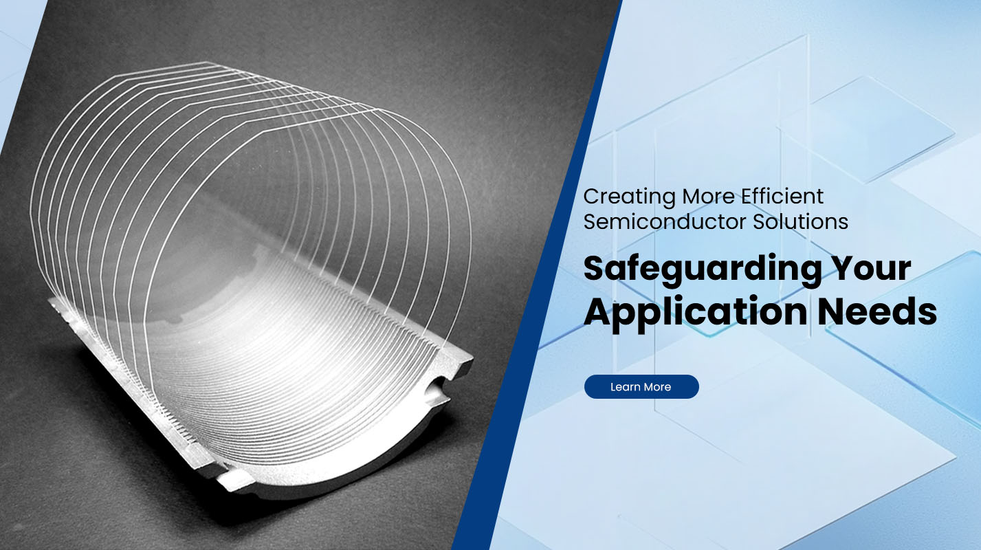
What Are Silicon Wafers Used For?
Silicon Wafers are the foundational material behind nearly all modern electronic technologies. From everyday consumer devices to advanced industrial systems, these thin, precisely engineered slices of silicon enable the performance, reliability, and scalability that today’s digital world demands. Understanding what silicon wafers are used for helps clarify why they remain irreplaceable in semiconductor manufacturing.
Core Role of Silicon Wafers in Semiconductors
At their most fundamental level, silicon wafers serve as the substrate on which integrated circuits are built. Through processes such as doping, photolithography, etching, and deposition, complex circuit patterns are formed directly on the wafer surface. Each wafer can contain hundreds or thousands of individual chips, which are later separated and packaged.
Silicon is favored because of its stable crystal structure, excellent electrical properties, and compatibility with high-volume manufacturing. These characteristics allow manufacturers to produce chips with consistent performance, tight tolerances, and high yields across large production runs.
Use in Integrated Circuits and Microprocessors
One of the most significant applications of silicon wafers is in integrated circuits and microprocessors. CPUs, GPUs, memory chips, and logic controllers all begin as silicon wafers. The wafer acts as a platform for billions of transistors, enabling complex computation, data storage, and signal processing.
As chip architectures advance toward smaller process nodes, wafer quality becomes even more critical. Uniform resistivity, low defect density, and precise thickness control directly influence device speed, power efficiency, and thermal stability.
Silicon Wafers in Power Electronics
Beyond logic and computing, silicon wafers are essential in power electronics. Devices such as power MOSFETs, IGBTs, and rectifiers rely on silicon substrates to manage high voltages and currents efficiently. These components are widely used in power supplies, electric vehicles, renewable energy systems, and industrial automation.
In power applications, wafer parameters such as crystal orientation, doping concentration, and breakdown voltage capability are carefully selected to balance efficiency, durability, and cost.
Applications in Sensors and MEMS Devices
Silicon wafers are also widely used in sensors and MEMS devices. Accelerometers, gyroscopes, pressure sensors, and micro-actuators are fabricated directly on silicon substrates. The mechanical strength and predictable behavior of silicon at micro scales make it ideal for combining mechanical structures with electronic control circuits.
These devices play a crucial role in smartphones, automotive safety systems, medical equipment, and industrial monitoring solutions.
Role in Photonics and Optoelectronics
In photonics and optoelectronics, silicon wafers support devices that interact with light, such as photodiodes, image sensors, and optical communication components. Silicon’s compatibility with CMOS processes allows optical and electronic functions to be integrated on the same wafer, improving performance and reducing system complexity.
This integration is particularly important in high-speed data transmission, imaging systems, and advanced sensing technologies.
Manufacturing, Research, and Custom Applications
Silicon wafers are not limited to mass production environments. They are also widely used in research institutions, pilot production lines, and custom engineering projects. Specialized wafers with unique diameters, orientations, or surface treatments enable experimentation, prototyping, and low-volume manufacturing for emerging technologies.
For companies seeking reliable wafer solutions across standard and customized requirements, manufacturers such as Plutosemi provide silicon wafer products designed to support both commercial production and advanced development needs. More information can be found at https://www.plutosemitech.com.
Common Silicon Wafer Applications Overview
| Application Area | Typical Use Case | Key Benefit of Silicon Wafers |
|---|---|---|
| Integrated Circuits | CPUs, memory, logic chips | High precision and scalability |
| Power Electronics | Inverters, converters, power control devices | Voltage and thermal stability |
| Sensors and MEMS | Motion, pressure, environmental sensing | Mechanical and electrical integration |
| Optoelectronics | Image sensors, photodiodes | CMOS compatibility |
| Research and Prototyping | New semiconductor technologies | Customizable material properties |
Why Silicon Wafers Remain Essential
Despite the emergence of alternative materials, silicon wafers continue to dominate the semiconductor industry. Their well-established supply chain, extensive process knowledge, and balanced performance characteristics make them the most practical and cost-effective choice for a wide range of applications.
As electronics continue to evolve toward higher integration, lower power consumption, and greater reliability, silicon wafers will remain at the core of innovation, supporting both current technologies and future breakthroughs.


