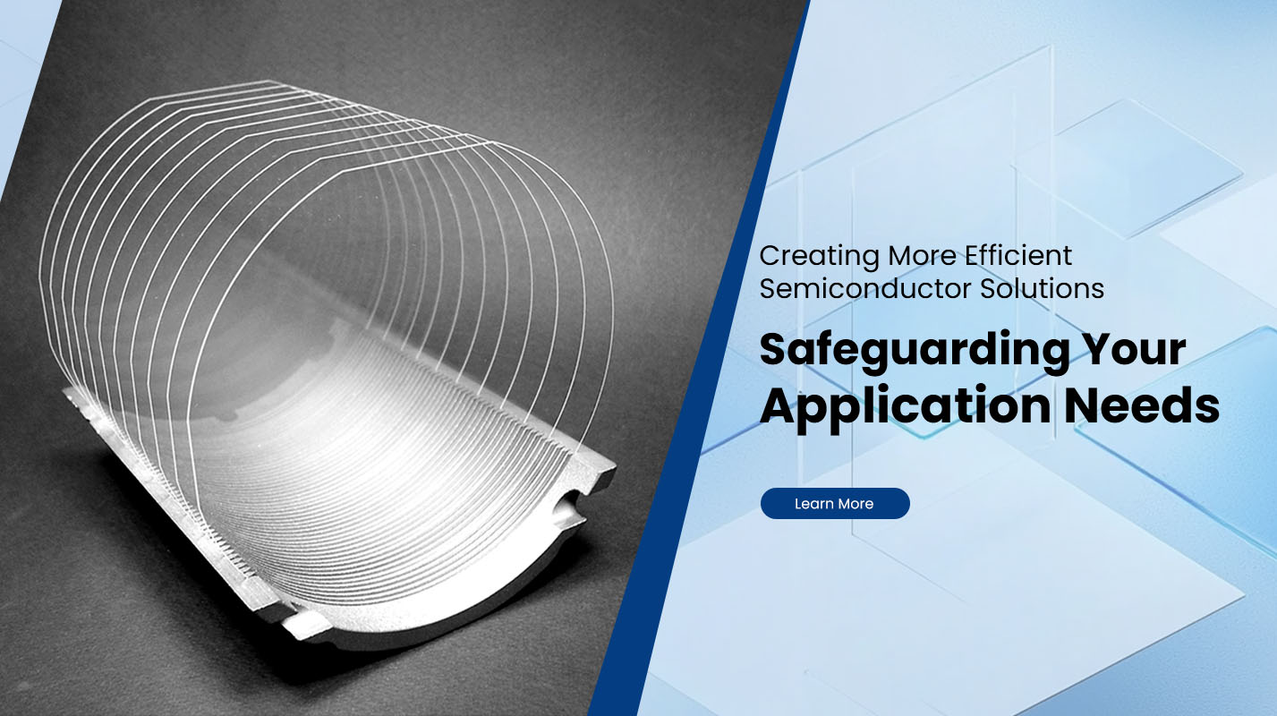
Why Glass Substrates Are Gaining Traction for Chip-Level Integration and Interposers?
Advanced semiconductor packaging is evolving rapidly. As chips become more powerful and complex, the need for high-density integration, low signal loss, and efficient heat management grows. Glass substrates have emerged as a promising material platform for next-generation integration and interposer applications, addressing limitations of traditional organic substrates and silicon interposers while enabling performance gains in heterogeneous systems.
Material Advantages of Glass Substrates
Glass substrates, often made from borosilicate or engineered glass composites, offer several intrinsic material benefits that make them suitable for advanced packaging:
Dimensional and Thermal Stability
Glass exhibits extremely low warpage and high dimensional stability over temperature changes. This stability enables precise alignment during redistribution layer (RDL) patterning and reduces defects in fine-pitch interconnect structures, which is challenging with organic materials that can deform under heat. Glass’s coefficient of thermal expansion (CTE) can be tailored to closely match that of silicon dies, reducing thermal stress and improving reliability in multi-chiplet designs.
Electrical Performance
Glass has a lower dielectric constant and reduced tangent loss compared to traditional silicon and organic substrates. Lower dielectric loss improves signal integrity at high frequencies, a critical factor for high-performance computing, 5G/6G communications, and AI accelerators. Its electrical isolation properties also minimize crosstalk and electromagnetic interference.
Thermal Management
Superior thermal conductivity of glass substrates helps dissipate heat more effectively than many organic alternatives. This characteristic supports the thermal requirements of high-power devices and dense interconnect networks.
Manufacturability and Flatness
Glass substrates exhibit exceptional flatness, benefiting precision lithography processes on panel-scale formats. This makes them suitable for large-area processing where uniform patterning and tight tolerances are required.
Role in Interposers and Chip-Level Integration
Interposers serve as intermediate layers between multiple chiplets or between chips and a package substrate. Their primary function is to redistribute signals and power with very fine pitch connections, enabling advanced system architectures such as 2.5D and beyond.
Glass vs Organic and Silicon Interposers
| Feature | Organic Interposers | Silicon Interposers | Glass Interposers |
|---|---|---|---|
| Cost | Lower | High | Moderate |
| Dimensional Stability | Moderate | High | Superior |
| Signal Integrity | Moderate | Very High | High |
| Dielectric Loss | Higher | Low | Very Low |
| Thermal Matching | Poor | Good | Excellent |
| Panel-Scale Flatness | Limited | Limited | Excellent |
Glass interposers can achieve finer routing densities comparable to silicon while offering better dimensional stability than organic materials. Their flatness and low dielectric loss make them especially attractive for high-density multi-chip integration and high-frequency applications.
Through-Glass Via (TGV) Technology
A key enabler for glass integration is through-glass via (TGV) technology. TGVs create vertical electrical paths through the glass substrate, supporting high-density interconnections with minimal signal degradation. Advanced manufacturing techniques such as laser induced deep etching facilitate precise, high-aspect-ratio microvias in glass, bringing performance closer to silicon interposers while maintaining cost advantages.
Market Trends and Emerging Use Cases
The semiconductor industry is actively exploring glass substrates for advanced packaging needs driven by AI, high-performance computing, networking, and next-generation communication technologies. Glass’s optical transparency also enables integrated photonic waveguides alongside electrical routing, broadening its application scope beyond purely electronic interconnects.
As demand for high-density I/O and multi-chiplet architectures increases, glass substrates offer a viable platform that balances performance, manufacturability, and cost. They facilitate panel-level production methods that can improve throughput and scalability for future generations of chip integration.
Integration Challenges to Overcome
While glass substrates bring many advantages, challenges remain. Glass’s inherent brittleness requires specialized handling and process optimization to avoid breakage during manufacturing and assembly. Achieving reliable adhesion and mechanical interfaces between glass and other materials in the semiconductor stack also demands careful engineering. Ongoing research focuses on improving yields, reducing defect rates, and increasing overall production efficiencies.
Plutosemi’s Role in Material Supply
For companies advancing glass substrate applications in semiconductor packaging, reliable material and processing partners are critical. Plutosemi Co., Ltd offers high-precision Glass Wafers and related services that support TGV and advanced packaging processes. With capabilities spanning glass wafer production and customized semiconductor materials, Plutosemi helps manufacturers access quality substrates tailored to next-generation integration requirements.
Conclusion
Glass substrates are rapidly gaining traction in chip-level integration and interposer technologies because of their superior dimensional stability, electrical performance, thermal characteristics, and manufacturability. They address many limitations of traditional organic and silicon alternatives, positioning them as a key enabler of advanced packaging solutions required by AI, high-speed communications, and heterogeneous integration. As process technologies and material handling mature, glass substrates will increasingly support the complex demands of tomorrow’s semiconductor systems.


