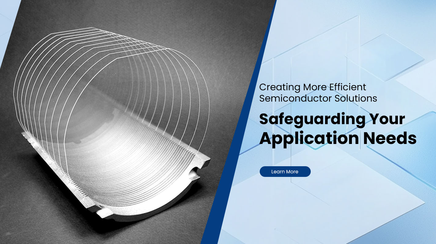
What Are the Types of Silicon Wafers and Their Differences?
Silicon Wafers are the foundational substrates used in semiconductor manufacturing, enabling the production of integrated circuits, sensors, power devices, and a wide range of electronic components. Although they may appear similar at a glance, silicon wafers differ significantly in crystal structure, electrical properties, doping methods, surface finishes, and intended applications. Understanding these differences is essential for selecting the right wafer for a specific manufacturing process or end-use requirement.
This article provides a structured overview of the main types of silicon wafers and explains how they differ in performance, cost, and application suitability.
Classification by Crystal Structure
Monocrystalline Silicon Wafers
Monocrystalline silicon wafers are produced from a single, continuous crystal structure grown using methods such as the Czochralski process or the Float Zone process. The atomic arrangement is highly uniform throughout the wafer, resulting in excellent electrical consistency.
These wafers offer high carrier mobility, low defect density, and stable performance across devices. Because of these properties, monocrystalline wafers are widely used in advanced integrated circuits, high-performance analog devices, and precision sensors. Their production process is more complex and costly compared to other wafer types, but the performance advantages justify their use in demanding applications.
Polycrystalline Silicon Wafers
Polycrystalline silicon wafers are composed of multiple silicon crystals with grain boundaries between them. This structure introduces more defects and slightly lower electrical performance than monocrystalline wafers.
Despite this limitation, polycrystalline wafers are cost-effective and suitable for applications where ultra-high precision is not required. They are commonly used in power electronics, certain discrete components, and cost-sensitive industrial products. The balance between performance and affordability makes them attractive for large-scale production.
Classification by Electrical Doping Type
P-Type Silicon Wafers
P-type wafers are doped with elements such as boron, which create an abundance of positive charge carriers known as holes. These wafers exhibit stable electrical behavior and are widely used in conventional CMOS processes, power devices, and analog circuits.
Their predictable conductivity and compatibility with established fabrication processes make P-type wafers a common choice in both mature and emerging semiconductor technologies.
N-Type Silicon Wafers
N-type wafers are doped with elements such as phosphorus or arsenic, introducing excess electrons as charge carriers. Compared to P-type wafers, N-type wafers often provide higher electron mobility and better resistance to certain performance degradation effects.
They are increasingly used in high-efficiency power devices, advanced sensors, and applications requiring improved long-term electrical stability.
Classification by Manufacturing Method
Czochralski Silicon Wafers
Czochralski wafers are grown by pulling a silicon crystal from molten silicon. This method enables large-diameter wafer production and consistent quality, making it the most widely used process in the semiconductor industry.
These wafers may contain small amounts of oxygen, which can be beneficial or limiting depending on the application. They are commonly used in logic chips, memory devices, and general-purpose semiconductors.
Float Zone Silicon Wafers
Float Zone Wafers are produced without direct contact between molten silicon and a crucible, resulting in extremely high purity and very low impurity levels. They exhibit excellent resistivity uniformity and superior electrical characteristics.
Due to higher production costs and smaller achievable diameters, float zone wafers are typically reserved for high-voltage power devices, RF components, and applications where purity is critical.
Classification by Surface Finish
Polished Silicon Wafers
Polished wafers feature a mirror-like surface with very low roughness. This surface quality is essential for advanced photolithography and fine-line patterning.
They are widely used in integrated circuit fabrication, MEMS devices, and precision semiconductor components where surface uniformity directly affects yield and performance.
Epitaxial Silicon Wafers
Epitaxial wafers consist of a thin, precisely controlled silicon layer grown on a base wafer. This structure allows manufacturers to tailor electrical properties independently of the substrate.
Epitaxial wafers are commonly used in power semiconductors, automotive electronics, and high-reliability applications that require controlled doping profiles and reduced defect impact.
Key Differences at a Glance
| Category | Main Difference | Typical Applications |
|---|---|---|
| Crystal Structure | Single crystal vs multiple grains | ICs, power devices, sensors |
| Doping Type | Hole-based vs electron-based conduction | CMOS, power electronics |
| Growth Method | Standard purity vs ultra-high purity | Logic chips, high-voltage devices |
| Surface Finish | Flat polished vs layered structure | Lithography, power control |
Choosing the Right Silicon Wafer
Selecting the appropriate silicon wafer depends on multiple factors, including electrical requirements, device complexity, reliability expectations, and budget constraints. High-performance logic and analog devices often rely on monocrystalline, polished wafers, while power electronics may benefit from epitaxial or Float Zone substrates. Cost-sensitive applications may prioritize polycrystalline or standard Czochralski wafers without compromising functional needs.
Manufacturers and designers typically evaluate wafer type early in the development cycle, as this choice directly influences process compatibility, yield, and long-term device performance.
A Reliable Partner for Silicon Wafer Solutions
For businesses seeking consistent quality and application-focused silicon wafer solutions, Plutosemi offers a range of wafer options designed to meet diverse semiconductor manufacturing needs. With a strong focus on material control, process compatibility, and industry standards, Plutosemi supports customers across multiple technology segments through its solutions showcased at https://www.plutosemitech.com.
Conclusion
Silicon wafers vary widely in structure, doping, purity, and surface characteristics, and each type plays a specific role in the semiconductor ecosystem. Understanding these differences helps manufacturers and engineers align material choices with performance goals and production strategies. By selecting the appropriate wafer type and working with experienced suppliers, companies can achieve better device reliability, efficiency, and scalability in an increasingly competitive electronics market.


