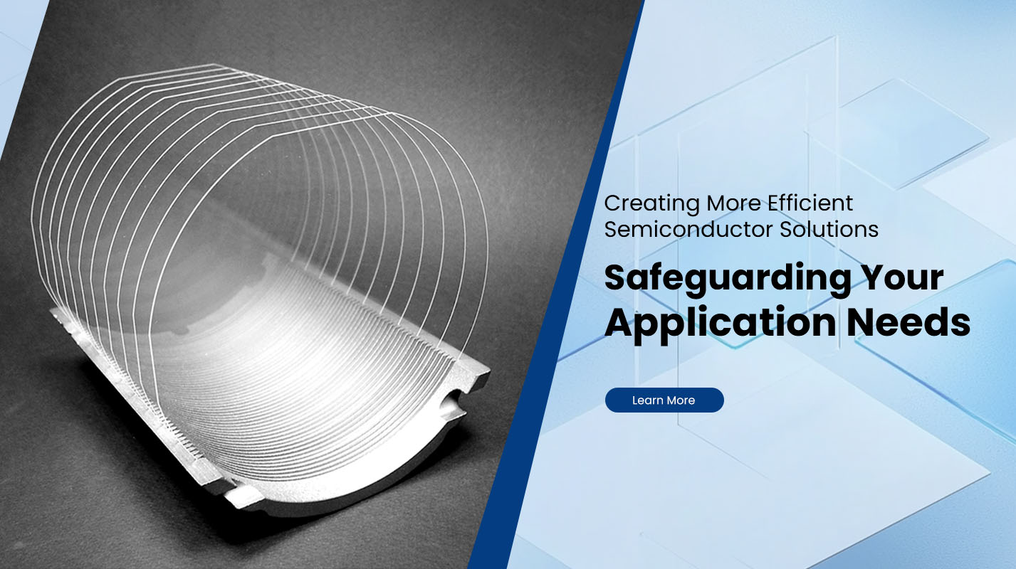
Cutting silicon wafers is one of the most delicate and crucial steps in semiconductor manufacturing. Precision in this stage directly affects the performance, yield, and integrity of microelectronic devices. Silicon wafers, typically ranging from 100 mm to 300 mm in diameter, are extremely thin and brittle, requiring specialized equipment, environmental control, and optimized cutting parameters to achieve clean, crack-free edges.
-
2025-11-07
-
2025-08-09Silicon wafers are the foundation of modern electronics, serving as the substrate for integrated circuits (ICs), solar cells, and other semiconductor devices. While industrial processes typically use precision machines like diamond saws for wafer dicing, manual cutting may be necessary for prototyping, research, or small-scale production.


