


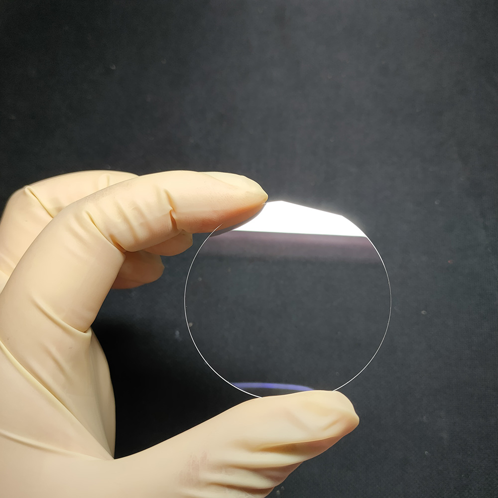
Single Crystal Sapphire Wafer
Sapphire Wafers

-
+86-17701852595 WhatsApp
-
sales@plutosemitech.com Email
sapphire wafers are primarily composed of aluminum oxide (Al₂O₃), which has a unique hexagonal crystal structure. This material exists naturally as the mineral sapphire and is artificially synthesized and processed into wafers. Its chemical properties are extremely stable, maintaining excellent chemical inertness even at high temperatures. In industrial production, the preparation of sapphire wafers requires a complex process involving crystal growth, cutting, grinding, and polishing to ensure high-precision dimensional and surface quality requirements. Due to its excellent physical and chemical properties, sapphire wafers play an indispensable role in numerous high-tech fields and are a key foundational material for the development of modern science and technology.

Single Crystal Sapphire Wafer Specifications
Products Standard:
| Product Name | Orientation | Standard Size | Thickness | Polishing |
| Sapphire substrate Sapphire wafer | < 0001> ±0.3° < 11-20 > ±0.3° < 10-10 > ±0.3° < 1-102 > ±0.3° Or other off-angle | 10x10mm 10x5mm 5x5mm 20x20mm 100x100mm Φ1" x 0.5mm Φ2" x 0.43mm Φ3" x 0.5mm Φ4" x 0.65mm Φ6" x 1.0mm Φ8" x 1.0mm Or others | 0.1mm 0.2mm 0.5mm 1.0mm 2.0mm Or others | Fine ground Single side polished Double side polished Roughness: Ra < 3A(0.3nm) (Epi-ready) |
Technical Specifications:
| Product Name | Sapphire single crystal substrate, Sapphire wafer, Al2O3 wafer | ||
| Crystal Structure | Hexagonal system | ||
| Orientation | C-plane (0001), A-plane (11-20), M-plane (10-10), R-plane (1-102) | ||
| Lattice Constant | a=4.748Å c=12.97Å | ||
| Density | 3.98(g/cm3) | ||
| Melting Point | 2040℃ | ||
| Mohs Hardness | 9 | ||
| Coefficient of Thermal expansion | 7.5 (x10-6/ oC) | ||
| Thermal conductivity | ⊥c | //c | |
| 23℃ | 0.055 | 26℃ 0.060 | |
| 77℃ | 0.04 | 70℃ 0.041 | |
| Dielectric Constant | ~ 9.4 @300K at A axis ~ 11.58@ 300K at C axis | ||
| Packing | Class-100 Clean bag, in class-1000 clean room | ||
| OEM/ODM | Accept | ||
| Compay Nature | China Manufacturers Suppliers Factory | ||
Single Crystal Sapphire Wafer Features
1. High Purity:
Single Crystal Sapphire Wafers are extremely pure, with an Al₂O₃ content exceeding 99.999%. This high-purity Sapphire Wafer effectively reduces the impact of impurities on performance, ensuring that impurities do not affect device performance and reliability in applications such as high-precision semiconductor manufacturing and optical device processing. This provides a solid material foundation for the production of high-end technology products.
2. High Flatness:
This product boasts exceptional surface flatness, with roughness controllable to the nanometer level. Through precision machining, the Sapphire Wafer surface achieves atomic-level flatness, which is crucial for semiconductor manufacturing and optical device processing, which require high-precision thin film deposition and photolithography processes. This high flatness ensures uniformity of the thin film, improves the resolution and accuracy of photolithography, and thus enhances product performance and quality.
3. High Dimensional Precision:
Single Crystal Sapphire Wafers feature exceptionally high dimensional accuracy, with diameter and thickness tolerances controlled within extremely tight limits. Applications such as semiconductor manufacturing and microelectromechanical systems (MEMS) place extremely high demands on wafer dimensional accuracy. High-precision Sapphire Wafers ensure accurate wafer alignment and processing during large-scale integrated circuit manufacturing, reducing device performance fluctuations caused by dimensional errors and improving product yield and consistency.
4. High Optical Performance:
Sapphire Wafers exhibit excellent optical performance, with excellent transmittance for visible light and some infrared light. Their optical transmittance is high, exceeding 90% within specific wavelength ranges. Furthermore, they exhibit low absorption and scattering, making them suitable for a wide range of applications in optical windows, optical sensors, optical communications, and other fields, meeting the stringent material requirements of high-precision optical systems.
5. High Thermal Stability:
Sapphire Wafers exhibit excellent thermal stability, maintaining stable physical and chemical properties even in high-temperature environments. With a melting point of 2040°C, Sapphire Wafer exhibits no deformation, cracking, or performance degradation during high-temperature processing and use. This makes it an irreplaceable advantage in high-temperature applications such as high-temperature infrared windows and high-temperature sensors, allowing it to withstand extreme thermal environments and ensure the proper functioning of equipment.
6. High Chemical Stability:
This product exhibits exceptional chemical stability, resisting attack by a wide range of chemicals. Even in harsh chemical environments such as strong acids, strong bases, and organic solvents, the Sapphire Wafer remains chemically stable, resisting chemical reactions or corrosion. This characteristic makes it valuable for applications in chemical sensors, biosensors, and chemical analysis instruments, enabling long-term stable operation in complex chemical environments, ensuring accurate and reliable measurements.
7. High Mechanical Strength:
Single Crystal Sapphire Wafer boasts high mechanical strength, with a Mohs hardness of 9, second only to diamond. This means it possesses high compressive, flexural, and impact strengths. During manufacturing and use, it can withstand significant mechanical stress and is not easily damaged. Sapphire wafers, with their high mechanical strength, can be used to manufacture high-strength mechanical components and wear-resistant parts, extending product life and reducing maintenance costs.
8. High Thermal Conductivity:
Sapphire wafers offer excellent thermal conductivity and high thermal conductivity. In electronic device and semiconductor manufacturing, these high thermal conductivity wafers effectively conduct heat from the inside of the device to the outside, providing excellent heat dissipation. This helps improve the stability and reliability of electronic devices, preventing damage or performance degradation caused by overheating, and is crucial for heat dissipation management in high-performance electronic devices.
Single Crystal Sapphire Wafer Process Flow
1. Raw Material Preparation:
The first step in producing a Single Crystal Sapphire Wafer is raw material preparation. High-purity alumina powder is selected as the raw material and undergoes a series of purification processes to ensure a purity of at least 99.999%. The purified alumina powder is sintered in a high-temperature furnace to form a dense alumina ceramic block. This process requires precise control of temperature and time to ensure the quality and performance of the ceramic block, providing a high-quality raw material foundation for subsequent crystal growth.
2. Crystal Growth:
The next step is crystal growth. Advanced crystal growth techniques such as the Kyropoulos method or the Czochralski method are employed. In the Kyropoulos method, the sintered alumina ceramic block is placed in a high-temperature furnace and melted under specific temperature and atmosphere conditions to form a melt. Then, by controlling the temperature gradient and growth rate, crystals from the melt slowly grow on a seed crystal, forming a single crystal sapphire. In the Czochralski method, a seed crystal is immersed in a melt and slowly pulled and rotated to grow a crystal on it. The entire crystal growth process requires precise control of multiple parameters, including temperature, atmosphere, and growth rate, to ensure crystal quality and dimensional accuracy.
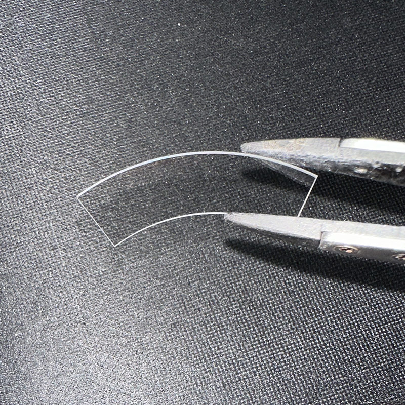
3. Crystal Processing:
After crystal growth is complete, the crystal processing stage begins. First, the grown single sapphire crystal is cut into the desired size and shape based on customer needs and product specifications. High-precision cutting equipment, such as laser cutters or diamond saws, is used during the cutting process to ensure cutting accuracy and surface quality. The cut crystals then undergo grinding and polishing to achieve the required surface flatness and roughness. This grinding and polishing process requires multiple iterations, with each step increasing in precision, ultimately achieving atomically flat surfaces on the Sapphire Wafer.
4. Inspection and Screening:
The processed Sapphire Wafers undergo rigorous inspection and screening. Advanced testing equipment, such as optical inspection instruments, X-ray diffractometers, and atomic force microscopes, comprehensively inspects Sapphire wafers for dimensional accuracy, surface flatness, crystal quality, and optical performance. During the testing process, wafers that fail to meet quality standards are screened and rejected, ensuring that every Sapphire wafer leaving the factory meets high quality standards. Statistical analysis of test data also provides a basis for optimizing and improving production processes, continuously improving product quality and consistency.
5. Packaging and Packaging:
The final step is the packaging and packaging process. Passing Sapphire wafers are packaged using moisture-proof, shock-proof, and anti-static packaging materials to ensure the safety and stability of the wafers during transportation and storage. Packaged Sapphire wafers are packaged according to customer requirements, and the packaging is labeled with product specifications, model numbers, quality standards, and other information for easy identification and handling. The entire packaging and packaging process is carried out strictly in accordance with standard operating procedures to ensure that the product maintains excellent quality and performance upon delivery to the customer.
Single Crystal Sapphire Wafer Application
1. Semiconductor Industry:
In semiconductor manufacturing, single crystal sapphire wafers are used as high-quality substrate materials. Due to their high purity, flatness, and dimensional accuracy, they provide an ideal substrate for growing semiconductor thin films. In the manufacture of semiconductor devices such as light-emitting diodes (LEDs) and microelectromechanical systems (MEMS), sapphire wafers ensure uniform thin film growth and excellent electrical properties, improving device luminous efficiency and stability. They are an indispensable key material in the semiconductor industry.
2. Optical Industry:
Sapphire wafers' high optical performance makes them widely applicable in the optical field. They can be processed into various optical components, such as optical windows, optical lenses, and optical sensors. For optical windows, sapphire wafers maintain excellent optical transmittance even in harsh environmental conditions and are used in applications such as infrared and ultraviolet windows. In optical sensors, sapphire wafers can serve as substrates for sensitive components, enhancing their sensitivity and stability and meeting the requirements of high-precision optical measurement and imaging.
3. Electronics:
In electronic devices, Sapphire Wafer's high thermal stability and high thermal conductivity make it an ideal heat sink material. It can be used to manufacture heat sinks and heat dissipation substrates for high-performance electronic devices, effectively dissipating heat generated by these devices and ensuring the stability and reliability of electronic devices under high-power operation. Furthermore, Sapphire Wafer's high chemical stability and mechanical strength make it crucial for encapsulating and protecting electronic devices, improving their corrosion and impact resistance.
4. Defense:
Sapphire Wafer holds strategic importance in the defense sector. Its high hardness, wear resistance, and impact resistance make it suitable for manufacturing high-strength military equipment components, such as armor and bulletproof glass. Furthermore, Sapphire Wafer's high optical performance and thermal stability make it widely applicable in military optical equipment and infrared detection equipment, improving the performance and operational effectiveness of military equipment and providing strong support for national defense security.
5. Scientific Research:
In scientific research, Sapphire Wafer is a crucial experimental material. It is widely used in research in physics, chemistry, materials science, and other fields. In physics experiments, Sapphire Wafer can be used to study the physical properties of crystals and quantum effects. In chemistry experiments, its high chemical stability makes it an ideal chemical reaction vessel and catalyst carrier. In materials science, Sapphire Wafer can serve as a substrate for research on new materials, supporting their development and application and promoting scientific and technological progress.
Packaging and Transportation
The packaging should be able to withstand the impact, vibration, stacking and extrusion that may be encountered during transportation, while also it has to easy to load, unload and handle.
We use professional wafer box packaging. The wafer box is protected by a double layer bag, the inside is a PE bag that can be dust-proof, and the outside is a aluminum foil bag that can be isolated from the air. The two-layer bags are vacuum-packed.
We will choose carton models according to different sizes of products. And between the product and the carton filled with shock-proof EPE foam, play a comprehensive protection.
Finally choose air transport to reach the customer's hands. This allows customers in any country and region to receive the product in the fastest time.
We comply with the Material Safety Data Sheet (MSDS) rules to ensure that the products transported are free of harmful substances and will not cause environmental pollution and explosion and other possible hazards.

Enterprise Strength
Factory Area: 3000 sq
Process:
1. Shaping→2. Edge Profile→3. Lapping→4. Polishing→5. Cleaning→6. Packing→7. Transportation
Capacity:
Glass Wafer --- 30K pcs
Silicon Wafer --- 20K pcs
(Equal to 6in)

Quality Assurance
Quality inspection method: Product inspection in accordance with SEMI standard or according to customer's requirements, together with product COA.
Warranty period: In accordance with the contract requirements.
Quality system management:
●Organize production according to ISO9001 and other quality system standards.
Quality management system and measures:
●Establish a strict quality assurance system, the heads of all departments and quality engineers to ensure the coordinated operation of the quality system.
●Strengthen the quality inspection system, strengthen the process quality control
●Strict material quality control, ensure that the input materials meet the design requirements and technical specifications.
●Implement a timely filing system for technical data to ensure that all processing technical data is complete/accurate.
Quality control in the production stage:
●Production preparation stage: carefully organize relevant personnel to learn product drawings and technical rules, and improve the technical level of employees.
●Quality control of the production process: the implementation of a strict handover system, the previous step of the process to the next step of the transfer, should be detailed processing. At the same time, strengthen the quality inspection system to ensure the quality of each step of the process.
●Quality acceptance: All processes must be quality acceptance before proceeding to the next process.

Pre-sales and After-sales
Pre-sales Service
Professional technical support and commercial team to help you determine product specifications according to product use, and issue specifications.
On-purchase Service
Produce products according to the confirmed specifications and our process.
After Sale Service
We will respond to any product problems encountered by customers or process problems encountered by customers within 24 hours. We can choose from various forms of service, such as email, video conference and so on.
Plutosemi Co., Ltd. was established in 2019, headquartered in Nanhai, Foshan, focusing on the research and development, production, and sales of high-performance semiconductor materials.
Advanced production capacity: We have three major production bases in China, with a monthly production capacity of 100000 equivalent 6-inch silicon wafers and 30000 equivalent 8-inch glass wafers, ensuring stable and efficient product supply for our customers.
High quality products: We provide efficient and stable product supply innovative solutions in the fields of glass wafers, silicon polishing wafers, epitaxial wafers (EPI), silicon on insulator wafers (SOI), and more. Our silicon wafers have the characteristics of ultra-thin, ultraflat, and high-precision, which can meet the needs of various high-end applications. Our glass and quartz substrates are also renowned for their high smoothness and precise aperture design.


