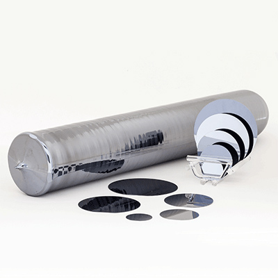
Semiconductor Dummy Silicon Wafer
Silicon Wafer

-
+86-17701852595 WhatsApp
-
sales@plutosemitech.com Email
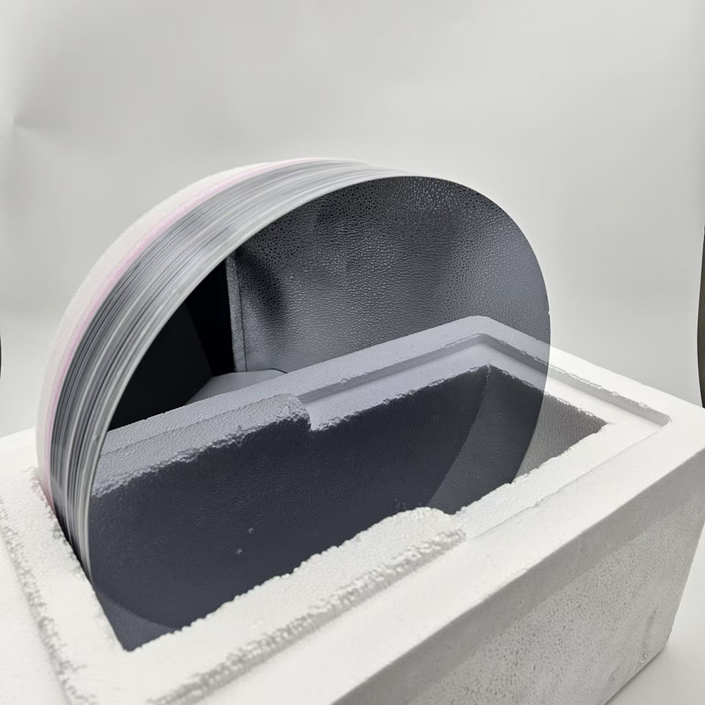
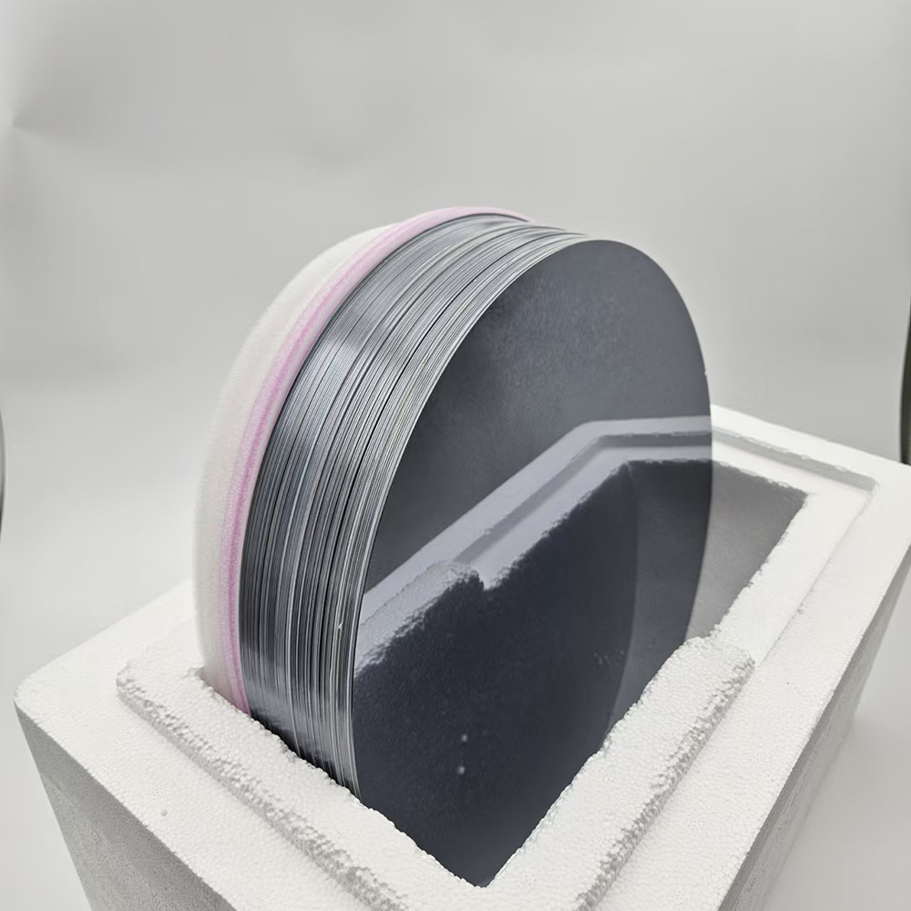
Dummy Silicon Wafer is a non-functional silicon wafer used in the semiconductor manufacturing process. It is mainly used to test and calibrate production equipment to ensure the stability and accuracy of the production line. This silicon wafer does not contain any integrated circuits and therefore will not be used in the final product, but its role in the manufacturing process is crucial. The use of Dummy Silicon Wafer helps reduce production costs and improve production efficiency while ensuring product quality. In the semiconductor industry, Dummy Silicon Wafer is an indispensable part that helps manufacturers optimize the production process without sacrificing the actual product.

Semiconductor Dummy Silicon Wafer Specifications
| Item | Specifications | ||
| Diameter | 150mm | 200mm | 300mm |
| Type | P/N | P/N | P/N |
| Notch | SEMI/JEIDA | Notch/OF | Notch |
| Thickness | 675±25/625±25μm | 725±25μm | 775±25μm |
| Frontside | Polished | Polished | Polished |
| Backside | Etched | Etched | Etched |
| OEM/ODM | Accept | ||
| Compay Nature | China Manufacturers Suppliers Factory | ||
Semiconductor Dummy Silicon Wafer Features
1. Various diameters
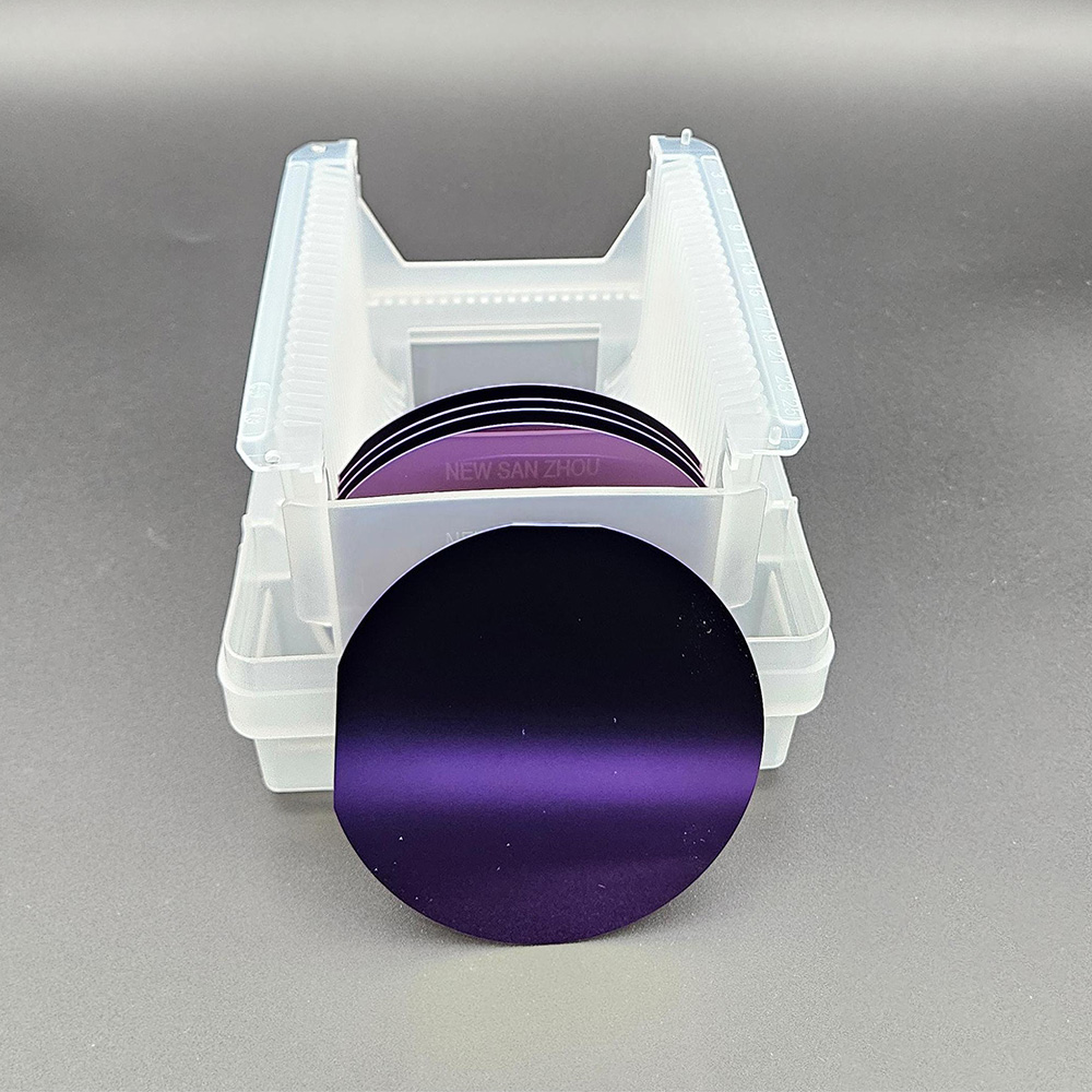
The diameters of Dummy Silicon Wafer provided by Plutosemi range from 150mm to 300mm, covering the mainstream semiconductor production needs. These sizes not only meet industry standards such as SEMI and JEITA, but also ensure compatibility with existing production line equipment, providing customers with a wide range of choices to meet different process requirements.
2. Double-sided processing
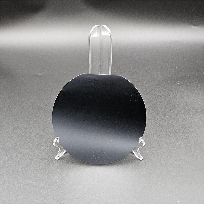
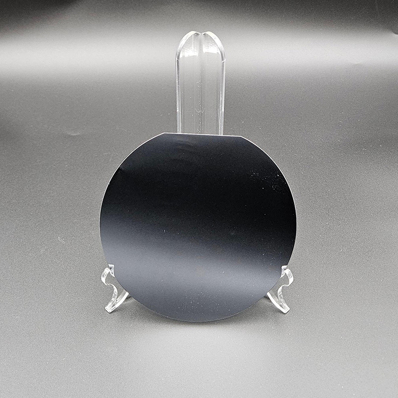
Dummy Silicon Wafer provides two surface treatment methods: polishing and etching. The front side uses high-precision polishing technology to ensure a smooth and flawless surface; the back side is etched to meet different testing and calibration needs. This double-sided processing technology not only improves the applicability of the product, but also enhances its performance in various applications.
3. Precise thickness
The thickness of Dummy Silicon Wafer is strictly controlled at 675±25μm, 725±25μm and 775±25μm. This precise thickness control is achieved through advanced manufacturing processes, ensuring stability and consistency in various applications, thereby improving the reliability of the production process.
4. Notchless design
Some Dummy Silicon Wafers adopt a notchless design, which is suitable for specific applications that require a complete silicon wafer, such as certain types of testing and calibration. The notchless design not only improves the durability of the product, but also ensures performance in specific applications, meeting the special needs of customers.
5. Standardized types
Two types of Dummy Silicon Wafers, P-type and N-type, are available to meet the needs of different semiconductor processes. This standardized design enables the product to be widely used in various semiconductor manufacturing processes, providing customers with flexible choices.
6. High quality control
All Dummy Silicon Wafers are produced in our own factories to ensure stable quality, and are tested by various test equipment for parameters to ensure product reliability. This strict quality control process ensures high standards and consistency of the products, providing customers with reliable products.
7. Fast delivery
Thanks to our own factories, Plutosemi is able to control delivery time and ensure that customers get the required Dummy Silicon Wafer in a timely manner. This fast delivery capability not only improves customers' production efficiency, but also reduces production delays caused by waiting for materials.
8. Flexible customization
Customized services are provided according to customer needs, including size, thickness and surface treatment, to meet specific application requirements. This flexible customization service enables Dummy Silicon Wafer to better adapt to the specific needs of customers and improve the applicability and competitiveness of the product.
Semiconductor Dummy Silicon Wafer Process Flow
1. Raw material selection
High-quality silicon materials are selected as raw materials to ensure the purity and consistency of the products. This high-quality raw material is the basis for producing high-quality Dummy Silicon Wafer and is essential to ensure product performance.
2. Cutting and polishing
The raw materials are processed into Dummy Silicon Wafers of the required size and surface quality through precision cutting and polishing processes. This precision processing technology not only improves the dimensional accuracy of the product, but also ensures the smoothness and consistency of the surface.
3. Thickness control
Advanced thickness control technology is used to ensure that the thickness of Dummy Silicon Wafer precisely meets the specification requirements. This precise thickness control is achieved through precise measurement and adjustment, ensuring the consistency and reliability of the product.
4. Surface treatment
According to customer needs, Dummy Silicon Wafer is polished or etched to achieve the desired surface characteristics. This surface treatment technology not only improves the applicability of the product, but also enhances its performance in various applications.
5. Quality inspection
Strict quality inspection is carried out during the production process to ensure that each piece of Dummy Silicon Wafer meets the quality standards. This strict quality inspection process ensures the high standards and consistency of the products and provides customers with reliable products.
6. Packaging and Storage
Use appropriate packaging and storage methods to protect Dummy Silicon Wafer from damage during transportation and storage. This proper packaging and storage method not only protects the product, but also ensures that it remains in the best condition when it reaches the hands of customers.
Semiconductor Dummy Silicon Wafer Application
1. Equipment calibration: The accuracy and stability of equipment are crucial in the semiconductor manufacturing process. Dummy Wafer, as an important tool for equipment calibration and verification, can simulate the operating status of real wafers in the equipment, helping engineers accurately evaluate the performance of the equipment. By using Dummy Wafer for equipment calibration, it is possible to ensure the accuracy of various parameters during the manufacturing process, thereby improving product quality and production efficiency.
2. Process optimization: Dummy Wafer plays a crucial role as a test sample in developing new processes or optimizing existing processes. Engineers can adjust and optimize various process parameters on Dummy Wafer, observe and analyze the impact of different parameters on the wafer manufacturing process. This Dummy Wafer based process optimization method can reduce the risk and cost of directly operating real wafers, while improving the efficiency and success rate of process development.
3. Production line testing: Regular testing on the production line is an important means of evaluating the stability and reliability of the production line. Dummy Wafer can be used as a test sample to simulate the operation process of real wafers on the production line, helping engineers discover problems and hidden dangers in the production line in a timely manner. Regular testing and evaluation of the production line can ensure its stable operation, improve product yield and production efficiency.
4. Training and teaching: For new employees, quickly familiarizing themselves with semiconductor manufacturing processes and operating standards is crucial. Dummy Wafer, as a teaching tool, can visually demonstrate the various stages and operational points in the wafer manufacturing process. Through practical operation of Dummy Wafer, new employees can gain a deeper understanding of the principles and processes of semiconductor manufacturing, and improve their operational skills and levels.
5. Quality control: Using Dummy Wafer in the quality control process can ensure that the product meets relevant standards and requirements. By conducting various tests and inspections on Dummy Wafer, the quality control effectiveness during the production process can be evaluated, and quality issues can be identified and corrected in a timely manner. This Dummy Wafer based quality control method can improve product quality and stability, enhance customer trust and satisfaction with the product.
Packaging and Transportation
The packaging should be able to withstand the impact, vibration, stacking and extrusion that may be encountered during transportation, while also it has to easy to load, unload and handle.
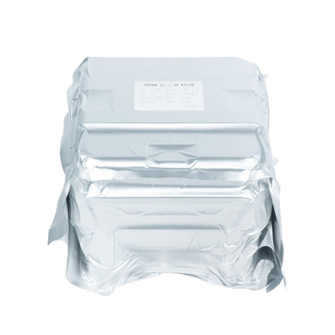
We use professional wafer box packaging. The wafer box is protected by a double layer bag, the inside is a PE bag that can be dust-proof, and the outside is a aluminum foil bag that can be isolated from the air. The two-layer bags are vacuum-packed.
We will choose carton models according to different sizes of products. And between the product and the carton filled with shock-proof EPE foam, play a comprehensive protection.
Finally choose air transport to reach the customer's hands. This allows customers in any country and region to receive the product in the fastest time.
We comply with the Material Safety Data Sheet (MSDS) rules to ensure that the products transported are free of harmful substances and will not cause environmental pollution and explosion and other possible hazards.

Enterprise Strength
Factory Area: 3000 sq
Process:
1. Shaping→2. Edge Profile→3. Lapping→4. Polishing→5. Cleaning→6. Packing→7. Transportation
Capacity:
Glass Wafer --- 30K pcs
Silicon Wafer --- 20K pcs
(Equal to 6in)

Quality Assurance
Quality inspection method: Product inspection in accordance with SEMI standard or according to customer's requirements, together with product COA.
Warranty period: In accordance with the contract requirements.
Quality system management:
●Organize production according to ISO9001 and other quality system standards.
Quality management system and measures:
●Establish a strict quality assurance system, the heads of all departments and quality engineers to ensure the coordinated operation of the quality system.
●Strengthen the quality inspection system, strengthen the process quality control
●Strict material quality control, ensure that the input materials meet the design requirements and technical specifications.
●Implement a timely filing system for technical data to ensure that all processing technical data is complete/accurate.
Quality control in the production stage:
●Production preparation stage: carefully organize relevant personnel to learn product drawings and technical rules, and improve the technical level of employees.
●Quality control of the production process: the implementation of a strict handover system, the previous step of the process to the next step of the transfer, should be detailed processing. At the same time, strengthen the quality inspection system to ensure the quality of each step of the process.
●Quality acceptance: All processes must be quality acceptance before proceeding to the next process.

Pre-sales and After-sales
Pre-sales Service
Professional technical support and commercial team to help you determine product specifications according to product use, and issue specifications.
On-purchase Service
Produce products according to the confirmed specifications and our process.
After Sale Service
We will respond to any product problems encountered by customers or process problems encountered by customers within 24 hours. We can choose from various forms of service, such as email, video conference and so on.
Plutosemi Co., Ltd. was established in 2019, headquartered in Nanhai, Foshan, focusing on the research and development, production, and sales of high-performance semiconductor materials.
Advanced production capacity: We have three major production bases in China, with a monthly production capacity of 100000 equivalent 6-inch silicon wafers and 30000 equivalent 8-inch glass wafers, ensuring stable and efficient product supply for our customers.
High quality products: We provide efficient and stable product supply innovative solutions in the fields of glass wafers, silicon polishing wafers, epitaxial wafers (EPI), silicon on insulator wafers (SOI), and more. Our silicon wafers have the characteristics of ultra-thin, ultraflat, and high-precision, which can meet the needs of various high-end applications. Our glass and quartz substrates are also renowned for their high smoothness and precise aperture design.